[Joe Colosimo] is putting on a show with his PCB business card project. The idea isn’t new, but his goal is to keep it simple and undercut the cost of all other PCB cards he’s seen. This is the third generation of the board design, and he’s just waiting on some solder mask solution before he tries running it through the reflow oven.
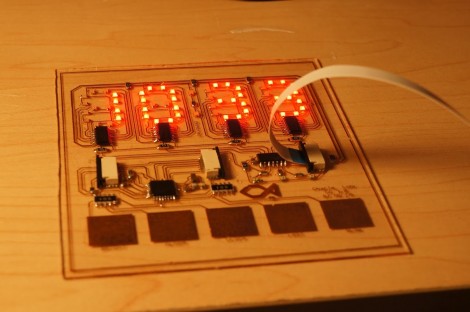
The first two prototypes used some through-hole parts. Notably, the battery was to be positioned in a circular cut-out and held in place by a metal strap and some bare wires. But he couldn’t quite get it to work right so this design will transition to a surface-mount strap for one side, and the large circular pad for the other. At each corner of the board there is a footprint for an LED. He tried milling holes in the board to edge-light the substrate. Now he just mounts the LED upside down to give the board a blue glow. The LEDs are driven by an ATtiny10 microcontroller which takes input from the touch sensor array at the bottom right.
He etched a QR code on the board which seems to work better than the milled QR experiments we saw back in April. The link at the top point’s to [Joe’s] main page on the card. Don’t forget to follow the links at the bottom which cover each part of the development more in-depth.
[Thanks Skitchin]