CO2 Laser Decapping To Fix Soldering Mistake

[Carsten] messed up. He was soldering an ARM CPU onto a quadcopter board in haste, failed to notice that the soldering iron was turned up to eleven, and pulled some of the traces up off the PCB. In the process of trying to fix that, he broke three pins off of the 100-pin CPU. The situation was going from bad to worse.

Instead of admitting defeat, or maybe reflowing the CPU off of the board, [Carsten] lasered the epoxy case off of the chip down to the lead frame and worked a little magic with some magnet wire. A sweet piece of work, to be sure!

Continue reading “CO2 Laser Decapping To Fix Soldering Mistake”

Using A Laser Cutter To Decap ICs

The black blob IC is of a particular annoyance to the modern hacker. There is no harm in peeking under the hood to see how the IC works. But when it’s covered in a mountain of seemingly indestructible epoxy, this can be a bit difficult. And such was the case for [Jamie], who had found an old electronic pocket dictionary whose main PC board boasted not one, but two of the black blob ICs.

ICThe lack of traces between the two pushed [Jamie’s] curiosity past the tipping point. He didn’t have access to any nitric acid which is used in the customary chemical decapping process. He did, however, have access to a laser cutter. It turns out that decapping ICs with a laser cutter is not only possible, it’s not that difficult.

100% power at 300mm per seconds on a cheap 40 Watt “eBay” laser cutter is all it takes. Three passes did the trick for [Jamie], but this will be dependent on the thickness of the black blob epoxy. Each case will likely be unique.

Got a laser cutter? Then take a peek at a few black blob ICs and let us know what you find.

Thanks to [ex-parrot] for the tip!

Looking Inside The KR580VM80A Soviet I8080 Clone

The folks at Zeptobars are on a roll, sometimes looking deep inside historic chips and at others exposing fake devices for our benefit. Behind all of those amazing die shots are hundreds of hours of hard work. [Mikhail] from Zeptobars recently tipped us off on the phenomenal work done by engineer [Vslav] who spent over 1000 hours reverse engineering the Soviet KR580VM80A – one of the most popular micro-controllers of the era and a direct clone of the i8080.

But before [Vslav] could get down to creating the schematic and Verilog model, the chip needed to be de-capped and etched. As they etched down, they created a series of high resolution images of the die. At the end of that process, they were able to determine that the chip had exactly 4758 transistors (contrary to rumors of 6000 or 4500). With the images done, they were able to annotate the various parts of the die, create a Verilog model and the schematic. A tough compatibility test confirmed the veracity of their Verilog model. All of the source data is available via a (CC-BY-3.0) license from their website. If this looks interesting, do check out some of their work that we have featured earlier like comparing real and fake Nordic dies and amazing descriptions of how they figure out the workings of these decapped chips. If this is too deep for you check out the slightly simpler but equally awesome process of delayering PCBs.

Reverse Engineering The Die Of A ULN2003 Transistor Array

uln2003-die-reverse-engineering

We’re no strangers to looking at uncapped silicon. This time around it’s not just a show and tell, as one transistor form a ULN2003 chip is reverse engineered.

The photo above is just one slice from a picture of the chip after having its plastic housing remove (decapped). It might be a stretch to call this reverse engineering. It’s more of a tutorial on how to take a functional schematic and figure out how each component is placed on a photograph of a chip die. Datasheets usually include these schematics so that engineers know what to expect from the hardware. But knowing what a resistor or transistor looks like on the die is another story altogether.

The problem is that you can’t just look at a two dimensional image like the one above. These semiconducting elements are manufactured in three dimensions. The article illustrates where the N and P type materials are located on the transistor using a high-res photo and a reference diagram.

If you want to photograph your own chip dies there are a few ways to decap them at home.

Boiling Acid Used To See Chip Die

When a project starts off by heating acid to its boiling point we say no thanks. But then again we’re more for the projects that use ones and zeros or a hot soldering iron. If you’re comfortable with the chemistry like [Michail] this might be right up your alley. He used boiling acid to expose and photograph the die from several integrated circuits.

The title of our feature is a play on words. In this case, die refers to the silicone on which the IC has been etched. To protect it the hardware manufacturer first attaches the metal pins to the die, then encapsulates it in plastic. [Michail] removes that plastic case by heating sulfuric acid to about 300 degrees Celsius (that’s 572 Fahrenheit) then submerges the chips in the acid inside of a sealed container for about forty minutes. Some of the larger packages require multiple trips through the acid bath. After this he takes detailed pictures of the die and uses post processing to color enhance them.

This isn’t the only way to get to the guts of a chip. We’ve seen nitric acid and even tree sap (in the form of bow rosin) do the trick.

Taking A Look At Decapped ICs

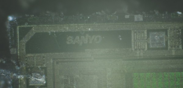
Aside from wanting to play around with nitric acid, [Ben] really didn’t have a reason to decap a few 74xx and 4000-series logic chips. Not that we mind, as he provides a great tutorial at looking at a bare IC that isn’t covered in epoxy and resin.

Most ICs are encased in a hard epoxy shell making it very difficult to look at the circuits within. [Ben] tried to grind this epoxy off with a Dremel tool, but didn’t have much luck until he moved over to a CNC mill to remove 0.040 – 0.050″ of epoxy without breaking the bond wires.

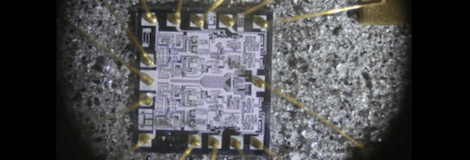
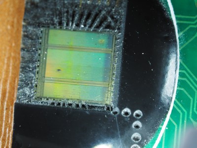
After carving out a nice pocket above the die, [Ben] put a few drops of nitric acid on the chip to dissolve the epoxy coating.  This worked very slowly at room temperature, but after putting the chips on a hot plate the acid was able to reveal the die underneath.

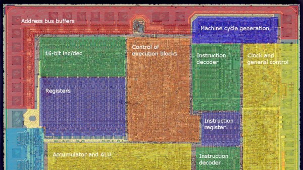
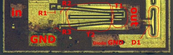
After successfully removing all the epoxy and giving them an acetone bath, [Ben] took his chips over to the microscope and was able to check out the underlying circuit. He doesn’t have any idea what he could do with these decapped logic chips, but the bond wires are still intact so he could still use these chips in a build.

We’d like to see a few decapped MEMS devices, but if you have a suggestion on what [Ben] can do with his decapped chips, drop a note in the comments.

Continue reading “Taking A Look At Decapped ICs”