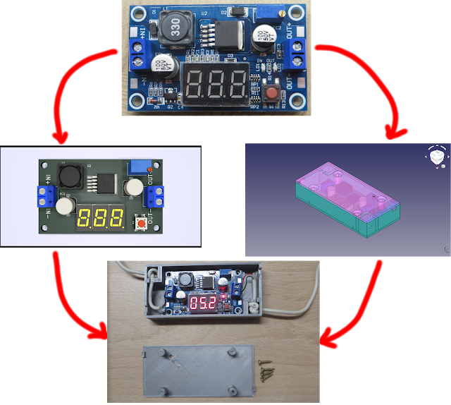
If you’ve used KiCad before, you’re certainly familiar with the handy 3D view that shows you a rendered view of what your assembled board would look like. But as [Vadim Panov] explains, you can take this capability a step further. With a few extra tools and a little bit of know-how, you can leverage KiCad’s PCB renderings to make custom 3D printable enclosures.
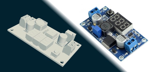
The first step is to design the PCB as you normally would in KiCad. This could be an original PCB of your own invention, or a digital representation of an off-the-shelf model you want to build an enclosure for. If the latter, then the PCB doesn’t need to be 100% accurate; the goal is really just to get the big components into roughly the right areas so you can get the clearances right. Though obviously you’ll want to make sure the board’s outer dimensions and mounting hole locations are recreated as accurately as possible.
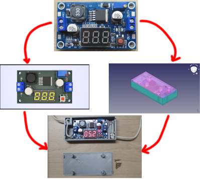 From there, [Vadim] recommends a tool called StepUp. This will take your PCB KiCad PCB files and create either a STEP or STL file of the assembled board which can be imported into your CAD package of choice. For the purposes of this demonstration he’s sticking with FreeCAD, as he likes the idea of it being a completely FOSS toolchain from start to finish.
Now that you have a model of the PCB in your CAD software, the rest is up to you. Naturally, there are existing enclosure models you can use such as the ones produced by the “Ultimate Box Maker” that we covered previously, but you could just as easily start building a new enclosure around the digital PCB.
Looking for a bit more guidance? As it so happens, our very own [Anool Mahidharia] will be presenting a class on how you can develop a KiCad + FreeCAD workflow as part of our recently launched HackadayU initiative.