Modern-day receivers are miracles of digital audio and video processing, but compared to their more analog brethren, they can come with a host of new and fascinating faults. The Onkyo TX-SA806 and SR806 receivers were released back in 2008, with [Tony359] recently getting the latter variant in for repair. Described as having weird digital distortion on the audio outputs, this particular issue got fixed by recapping the PCB with all the digital processing in the first video on this receiver, but this left the second issue unaddressed of a persistent hum, which is the topic of the second video on this repair.
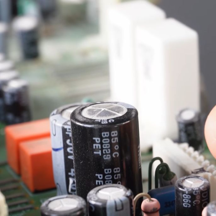
With the easy fix of recapping of the digital board already tried, next was a deep-dive into the receiver’s schematics to figure out where this low-frequency hum was coming from. With it sounding very much like mains frequency hum bleeding through, this was the starting point. Presumably somewhere on the power rails the normal filtering had broken down, so all rails had to be identified and checked for this interference.
With ripple on the 10V and 12V rails as well as the others seemingly in order, it wasn’t clear where the 100 Hz hum was coming from, but people on the BadCaps forum offered some help. After some back and forth it was deduced that the problem was the +15 VA rail, with heavy ripple on it due to a dead capacitor on the +22 V rail that comes straight from a transformer.
Continue reading “Fixing An Onkyo Receiver With Multiple Faults”