Mowing The Lawn With Lasers, For Science

Cutting grass with lasers works great in a test setup. (Credit: Allen Pan, YouTube)

Wouldn’t it be cool if you could cut the grass with lasers? Everyone knows that lasers are basically magic, and if you strap a diode laser or two to a lawn mower, it should slice through those pesky blades of grass with zero effort. Cue [Allen Pan]’s video on doing exactly this, demonstrating in the process that we do in fact live in a physics-based universe, and lasers are not magical light sabers that will just slice and dice without effort.

The first attempt to attach two diode lasers in a spinning configuration like the cutting blades on a traditional lawn mower led to the obvious focusing issues (fixed by removing the focusing lenses) and short contact time. Effectively, while these diode lasers can cut blades of grass, you need to give them some time to do the work. Naturally, this meant adding more lasers in a stationary grid, like creating a Resident Evil-style cutting grid, only for grass instead of intruders.

Does this work? Sort of. Especially thick grass has a lot of moisture in it, which the lasers have to boil off before they can do the cutting. As [Allen] and co-conspirator found out, this also risks igniting a lawn fire in especially thick grass. The best attempt to cut the lawn with lasers appears to have been made two years ago by [rctestflight], who used a stationary, 40 watt diode laser sweeping across an area. When placed on a (slowly) moving platform this could cut the lawn in a matter of days, whereas low-tech rapidly spinning blades would need at least a couple of minutes.

Obviously the answer is to toss out those weak diode lasers and get started with kW-level chemical lasers. We’re definitely looking forward to seeing those attempts, and the safety methods required to not turn it into a laser safety PSA.

Continue reading “Mowing The Lawn With Lasers, For Science”

A Windows Control Panel Retrospective Amidst A Concerning UX Shift

Once the nerve center of Windows operating systems, the Control Panel and its multitude of applets has its roots in the earliest versions of Windows. From here users could use these configuration applets to control and adjust just about anything in a friendly graphical environment. Despite the lack of any significant criticism from users and with many generations having grown up with its familiar dialogs, it has over the past years been gradually phased out by the monolithic Universal Windows Platform (UWP) based Settings app.

Whereas the Windows control panel features an overview of the various applets – each of which uses Win32 GUI elements like tabs to organize settings – the Settings app is more Web-like, with lots of touch-friendly whitespace, a single navigable menu, kilometers of settings to scroll through and absolutely no way to keep more than one view open at the same time.

Unsurprisingly, this change has not been met with a lot of enthusiasm by the average Windows user, and with Microsoft now officially recommending users migrate over to the Settings app, it seems that before long we may have to say farewell to what used to be an intrinsic part of the Windows operating system since its first iterations. Yet bizarrely, much of the Control Panel functionality doesn’t exist yet in the Settings app, and it remain an open question how much of it can be translated into the Settings app user experience (UX) paradigm at all.

Considering how unusual this kind of control panel used to be beyond quaint touch-centric platforms like Android and iOS, what is Microsoft’s goal here? Have discovered a UX secret that has eluded every other OS developer?

Continue reading “A Windows Control Panel Retrospective Amidst A Concerning UX Shift”

The BioHome3D by University of Maine.

3D Printed Homes Are All The Hype, But What Is Their Real Impact?

Additive manufacturing (AM) has been getting a lot of attention over the years, with its use in construction a recurring theme. Generally this brings to mind massive 3D printers that are carted to construction sites and assemble entire homes on the spot. That’s the perspective with which a recent ZDNet article by [Rajiv Rao] opens, before asking whether AM in construction is actually solving any problems. As [Rajiv] notes, the main use of such on-site AM construction is for exclusive, expensive designs, such as ICON’s House Zero which leans into the extruded concrete printing method.

Their more reasonable Wolf Ranch residential homes in Texas also use ICON’s Vulcan II printer to print walls out of concrete, with a roof, electrical wiring, plumbing, etc. installed afterwards. Prices for these Wolf Ranch 3 to 4 bedroom houses range from about $450,000 to $600,000, and ICON has been contracted by NASA to work a way to 3D print structures on the Moon out of regolith.

3D printed home by WASP out of clay. (Credit: WASP)

Naturally, none of these prices are even remotely in the range of the first-home buyers, or the many economically disadvantaged who make up a sizable part of the population in the US and many other nations in the Americas, Africa, etc. To make AM in construction economically viable, it would seem that going more flatpack and on-site assembly is the way to go, using the age-old pre-fabrication (prefab) method of constructions.

This is the concept behind the University of Maine’s BioHome3D, which mainly uses PLA, wood fiber and similar materials to create modules that contain insulation in the form of wood fiber and cellulose. These modules are 3D printed in a factory, after which they’re carted off to the construction site for assembly, pretty much like any traditional prefab home, just with the AM step and use of PLA rather than traditional methods.

Prefab is a great way to speed up construction and already commonly used in the industry, as modules can have windows, doors, insulation, electrical wiring, plumbing, etc. all installed in the factory, with on-site work limited to just final assembly and connecting the loose bits. The main question thus seems to be whether AM in prefab provides a significant benefit, such as in less material wasted by working from (discarded) wood pulp and kin.

While in the article [Rajiv] keeps gravitating towards the need to use less concrete (because of the climate) and make homes more affordable through 3D printing, AM is not necessarily the panacea some make it out to be, due to the fact that houses are complex structures that have to do much more than provide a floor, walls and a roof. If adding a floor (or two) on top of the ground floor, additional requirements come into play, before even considering aspects like repairability which is rarely considered in the context of AM construction.

New 2 GB Raspberry Pi 5 Has Smaller Die And 30% Lower Idle Power Usage

Recently Raspberry Pi released the 2GB version of the Raspberry Pi 5 with a new BCM2712 SoC featuring the D0 stepping. As expected, [Jeff Geerling] got his mitts on one of these boards and ran it through its paces, with positive results. Well, mostly positive results — as the Geekbench test took offence to the mere 2 GB of RAM on the board and consistently ran out of memory by the multi-core Photo Filter test, as feared when we originally reported on this new SBC. Although using swap is an option, this would not have made for a very realistic SoC benchmark, ergo [Jeff] resorted to using sysbench instead.

Naturally some overclocking was also performed, to truly push the SoC to its limits. This boosted the clock speed from 2.4 GHz all the way up to 3.5 GHz with the sysbench score increasing from 4155 to 6068. At 3.6 GHz the system wouldn’t boot any more, but [Jeff] figured that delidding the SoC could enable even faster speeds. This procedure also enabled taking a look at the bare D0 stepping die, revealing it to be 32.5% smaller than the previous C1 stepping on presumably the same 16 nm process.

Although 3.5 GHz turns out to be a hard limit for now, the power usage was interesting with idle power being 0.9 watts lower (at 2.4 W) for the D0 stepping and the power and temperatures under load also looked better than the C1 stepping. Even when taking the power savings of half the RAM versus the 4 GB version into account, the D0 stepping seems significantly more optimized. The main question now is when we can expect to see it appear on the 4 and 8 GB versions of the SBC, though the answer there is likely ‘when current C1 stocks run out’.

IBM’s Latest Quantum Supercomputer Idea: The Hybrid Classical-Quantum System

Although quantum processors exist today, they are still a long way off from becoming practical replacements for classical computers. This is due to many practical considerations, not the least of which are factors such as the need for cryogenic cooling and external noise affecting the system necessitating a level of error-correction which does not exist yet. To somewhat work around these limitations, IBM has now pitched the idea of a hybrid quantum-classical computer (marketed as ‘quantum-centric supercomputing’), which as the name suggests combines the strengths of both to create a classical system with what is effectively a quantum co-processor.

IBM readily admits that nobody has yet demonstrated quantum advantage, i.e. that a quantum computer is actually better at tasks than a classical computer, but they figure that by aiming for quantum utility (i.e. co-processor level), it could conceivably accelerate certain tasks for a classical computer much like how a graphics processing unit (GPU) is used to offload everything from rendering graphics to massively parallel computing tasks courtesy of its beefy vector processing capacity. IBM’s System Two is purported to demonstrate this when it releases.

What the outcome here will be is hard to say, as the referenced 2023 quantum utility demonstration paper involving an Ising model was repeatedly destroyed by classical computers and even trolled by a Commodore 64-based version. Thus, at the very least IBM’s new quantum utility focus ought to keep providing us with more popcorn moments like those, and maybe a usable quantum system will roll out by the 2030s if IBM’s projected timeline holds up.

Hardware Bug In Raspberry Pi’s RP2350 Causes Faulty Pull-Down Behavior

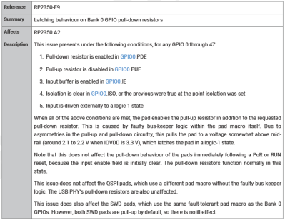
Erratum RP2350-E9 in the RP2350 datasheet, detailing the issue.

The newly released RP2350 microcontroller has a confirmed new bug in the current A2 stepping, affecting GPIO pull-down behavior. Listed in the Raspberry Pi RP2350 datasheet (page 1340) as erratum RP2350-E9, it involves a situation where a GPIO pin is configured as a pull-down with input buffer enabled. After this pin is then driven to Vdd (e.g. 3.3V) and then disconnected, it will stay at around 2.1 – 2.2 V for a Vdd of 3.3V. This issue was discovered by [Ian Lesnet] of [Dangerous Prototypes] while working on an early hardware design using this MCU.

The suggested workaround by Raspberry Pi is to enable the input buffer before a read, and disable it again immediately afterwards. Naturally, this is far from ideal workaround, and the solution that [Ian] picked was to add external pull-down resistors. Although this negates the benefits of internal pull-down resistors, it does fix the issue, albeit with a slightly increased board size and BOM part count.

As for the cause of the issue, Raspberry Pi engineer [Luke Wren] puts the blame on an external IP block vendor. With hindsight perhaps running some GPIO validation tests involving pull-up and pull-down configurations with and without input buffer set could have been useful, but we’re guessing they may be performed on future Pi chips. Maybe treating the RP2350 A0 stepping as an ‘engineering sample’ is a good idea for the time being, with A3 (or B0) being the one you may want to use in actual production.

In some ways this feels like déjà vu, as the Raspberry Pi 4 and previous SBCs had their own share of issues that perhaps might have been caught before production.

(Note: original text listed A0 as current stepping, which is incorrect. Text has been updated correspondingly)

DEC’s LAN Bridge 100: The Invention Of The Network Bridge

DEC’s LAN Bridge 100 was a major milestone in the history of Ethernet which made it a viable option for the ever-growing LANs of yesteryear and today. Its history is also the topic of a recent video by [The Serial Port], in which [Mark] covers the development history of this device. We previously covered the LANBridge 100 Ethernet bridge and what it meant as Ethernet saw itself forced to scale from a shared medium (ether) to a star topology featuring network bridges and switches.

Featured in the video is also an interview with [John Reed], a field service network technician who worked at DEC from 1980 to 1998. He demonstrates what the world was like with early Ethernet, with thicknet coax (10BASE5) requiring a rather enjoyable way to crimp on connectors. Even with the relatively sluggish 10 Mbit of thicknet Ethernet, adding an Ethernet store and forward bridge in between two of these networks required significant amounts of processing power due to the sheer number of packets, but the beefy Motorola 68k CPU was up to the task.

To prevent issues with loops in the network, the spanning tree algorithm was developed and implemented, forming the foundations of the modern-day Ethernet LANs, as demonstrated by the basic LAN Bridge 100 unit that [Mark] fires up and which works fine in a modern-day LAN after its start-up procedure. Even if today’s Ethernet bridges and switches got smarter and more powerful, it all started with that first LAN Bridge.

Continue reading “DEC’s LAN Bridge 100: The Invention Of The Network Bridge”