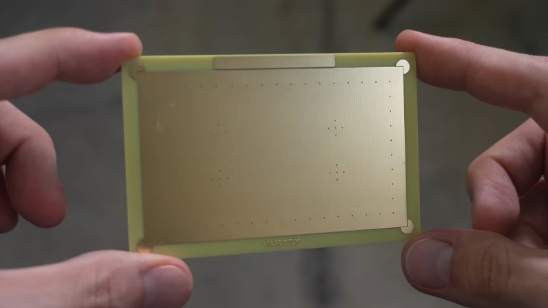
One of [CNLohr]’s bigger claims to fame is his process for making glass PCBs. They’re pretty much identical to regular, fiberglass-based PCBs, but [CNLohr] is building circuits on microscope slides. We’ve seen him build a glass PCB LED clock and a Linux Minecraft Ethernet thing, but until now, [CNLohr]’s process of building these glass PCBs hasn’t been covered in the depth required to duplicate these projects.
At the highest level of understanding, [CNLohr]’s glass PCBs really aren’t any different from traditional homebrew PCBs made on copper clad board. There’s a substrate, and a film of copper that is etched away to produce traces and circuits. The devil is in the details, and there are a lot of details for this build. Let’s dig deeper.
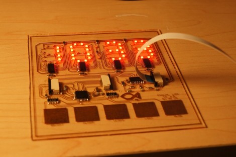
This clock looks fantastic because of the glass PCB used for the build. This banner image allows you to see all the traces and components, but when it is lifted off of the desk surface the LEDs which make up the 7-segment digits appear to be floating.
The concept isn’t new, but it’s a much larger format than we’ve seen before. When we first looked at [CNLohr’s] glass PCB fabrication he was using microscope slides. This uses a much larger pane of glass but it seems the fabrication still uses copper foil glued to the glass, then toner transfer etched like normal.
Here he’s testing out some 74LV164 chips as constant current drivers. One of the commenters on the Reddit thread is skeptical about using the chip in this way and so are we. But as the video after the break shows, it seems to work (at least for now). [CNLohr] also mentions that the AVR soldered on the display is burnt out which doesn’t help his case. Still, we love the look and can’t wait to see where he goes from here!
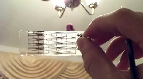
Our friend [Jeri] tipped us off about this cool video on youtube where the author makes his own “transparent” PCB’s using some nontraditional materials. One ounce copper foil is found online along with some clear glass microscope slides, from there it is just a matter of cementing the foil onto the glass slides with some thin UV curing glue. Once the 2 parts are mated the entire thing is popped into an eeprom eraser for its intense UV light, then excess is trimmed.
The normal routine of toner transfer is used to copy a circuit pattern onto the copper clad glass and it’s etched in standard ferric chloride. The copper is removed but the UV glue that was holding it is still left, some special care needs be followed as this stuff is pretty weak against even mild solvents, and you do not want your traces peeling up. Next no clean solder paste is applied and parts are soldered down with a heat gun, keeping the glass evenly heated to prevent it from cracking.
This leaves you with a board that looks like frosted glass, and in order to protect the glue while clearing up the frosted effect, some polyurethane is applied which fills in all the little bumps and smoothes the surface bout out to almost 100% clear.
The end application in this video is a touch sensitive board which works fine though the back side of the glass and presents a nice smooth interface for the user. Join us after the break for the video.
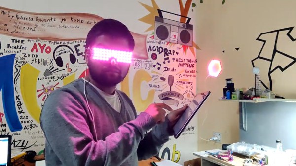
The design intelligently makes use of PCBs to form the entire structure of the glasses. One PCB makes up the left arm of the glasses, carrying an ESP12F microcontroller and the requisite support circuitry. It’s fitted to the front PCB through a slot, and soldered in place. The V+, GND, and DATA connections for the WS2812B LEDs also serve as the mechanical connection. The right arm of the glasses is held on in the same way, being the same as the left arm PCB but simply left unpopulated. A little glue is also used to stiffen up the connection.
Glass-based substrates are slowly beginning to push out organic substrates – as also commonly used in PCBs – due to often superior material properties for packaging. One area where glass substrates have however struggled is with through-hole vias and providing the conductive copper path through them. A 2024 article by [Keith Best] gives a good overview of the topic, with recent news showing how much companies like Intel are pushing for glass substrates, specifically for the packaging of dies.
One major advantage with vias in glass substrates is that they can be much smaller, enabling smaller than 0.1 mm diameter holes with far finer pitch. The challenge here is to make perfect holes with a laser that are defect-free, as well as have the intended diameter.
After that this through-glass via (TGV) has to be coated or filled with copper, much like their organic equivalent. Said TGV can be fully filled with copper, or use plating and add dielectric filler. Detecting flaws in such a finished TGV is important.
In a 2025 review article of glass substrate technologies by [Pratik Nimbalkar] et al. published in Chips the state of the art at the time was covered. The need for ever higher-density integration options with ASICs is highlight here, especially now that many chips today consist of multiple interconnected dies inside a single package.
The complications of creating TGVs with femtosecond laser pulses in Borofloat 33 glass are highlighted by [Daniel Franz] et al. in a 2025 research article, with microcracks and backside ablation observed without proper precautions, something which previously was often resolved by an etching step following said laser drilling. The main issue here is the post-drilling residual stress from the thermal shock, which the authors demonstrate can be largely prevented with careful tweaking of the laser drilling parameters.
As pointed out in a 2024 review article by [Chen Yu] et al. glass substrates are useful for far more than just high-density chip packaging. Glass substrates are also chemically resistant, have a higher heat resistance, are largely transparent to RF and can be hermetically sealed against outside influences. This makes them great for various advanced sensors and communication devices.
Meanwhile, if you wanted to do some metal-depositing on glass at home, we covered this recently.
Connected devices are ubiquitous in our era of wireless chips heavily relying on streaming data to someone else’s servers. This sentence might already start to sound dodgy, and it doesn’t get better when you think about today’s smart glasses, like the ones built by Meta (aka Facebook).
[sh4d0wm45k] doesn’t shy away from fighting fire with fire, and shows you how to build a wireless device detecting Meta’s smart glasses – or any other company’s Bluetooth devices, really, as long as you can match them by the beginning of the Bluetooth MAC address.
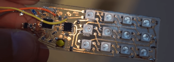
[sh4d0wm45k]’s device is a mini light-up sign saying “GLASSHOLE”, that turns bright white as soon as a pair of Meta glasses is detected in the vicinity. Under the hood, a commonly found ESP32 devboard suffices for the task, coupled to two lines of white LEDs on a custom PCB. The code is super simple, sifting through packets flying through the air, and lets you easily contribute with your own OUIs (Organizationally Unique Identifier, first three bytes of a MAC address). It wouldn’t be hard to add such a feature to any device of your own with Arduino code under its hood, or to rewrite it to fit a platform of your choice.
We’ve been talking about smart glasses ever since Google Glass, but recently, with Meta’s offerings, the smart glasses debate has reignited. Due to inherent anti-social aspects of the technology, we can see what’d motivate one to build such a hack. Perhaps, the next thing we’ll see is some sort of spoofed packets shutting off the glasses, making them temporarily inoperable in your presence in a similar way we’ve seen with spamming proximity pairing packets onto iPhones.
You know those old cliche that the younger generations have begun to cynically despise: “follow your dreams!” “You can be anything you put your mind to!” — well, perhaps they are true on occasion. For instance when [rctestflight] had PCBs that dreamed of becoming a hydrofoil, he found a way to make that dream come true.
It’s kind of obvious in retrospect: printed circuit boards are made of FR4, which is a form of fiberglass, and you know what else is commonly made of fiberglass? Boats. So yes, the material is suited for this task. The fact that solder joints hold up to use in a little remote-control hydrofoil is less obvious, but good to know. It certainly makes for easier assembly for those of us who have developed an allergy to epoxy.
Ease of assembly wasn’t really the point here: the point was that by making the “mast” of the hydrofoil out of PCB– that’s the part that holds the underwater wing– [rctestflight] figured he could (shock!) print a circuit onto it. Specifically, a liquid-level sensor, and because microcontrollers are so cheap these days he went the “total overkill” route of embedding an ESP32 on each mast. He started with a resistive sensor, but since those self-corrode too quickly, the team switched to a capacitive sensor that doesn’t need to form a galvanic cell in salt water. Come to think of it, that might still be a problem with the solder joint between the PCBs. Good thing nobody will be riding this one.
Having such a sensor and brain close-coupled allows for a faster control loop than the sonar [rctestflight] had previously been using to control his hydrofoil’s altitude.. Pivoting each mast with its own servo made for a smooth flight over the water— well, once they got the PID tuning set, anyway. Check it out in the video embedded below.