For those of us devoted to keeping an older vehicle on the road, the struggle is real. We know that at some point, a part will go bad and we’ll learn that it’s no longer available from the dealer or in the aftermarket, at least at a reasonable cost. We might get lucky and find a replacement at the boneyard, but if not — well, it was nice knowing ya, faithful chariot.
It doesn’t have to be that way, though, at least if the wonky part is one of the many computer modules found in most cars made in the last few decades. Sometimes they can be repaired, as with this engine control module from a Ford F350 pickup. Admittedly, [jeffescortlx] got pretty lucky with this module, which with its trio of obviously defective electrolytics practically diagnosed itself. He also had the advantage of the module’s mid-90s technology, which still relied heavily on through-hole parts, making the repair easier.
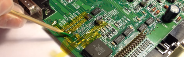
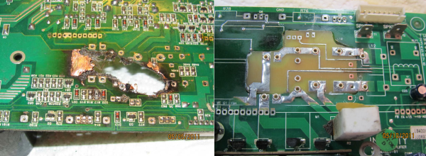
Unfortunately, his luck stopped there, as the caps had released the schmoo and corroded quite a few traces on the PCB. Complicating the repair was the conformal coating on everything, a common problem on any electronics used in rough environments. It took a bit of probing and poking to locate all the open traces, which included a mystery trace far away from any of the leaky caps. Magnet wire was used to repair the damaged traces, the caps were replaced with new ones, and everything got a fresh coat of brush-on conformal coating.
Simple though they may be, we really enjoy these successful vehicle module repairs because they give us hope that when the day eventually comes, we’ll stand a chance of being able to perform some repair heroics. And it’s nice to know that something as simple as fixing a dead dashboard cluster can keep a car out of the crusher.
Continue reading “Simple PCB Repairs Keep Old Vehicle Out Of The Crusher”