Here at Hackaday HQ, we all have opinions about the way we like to do things. And no surprise, this extends to the way we like to lay out circuits in schematics. So when we were discussing our own takes on this piece on suggested schematic standards, it was maybe more surprising how much we did agree on than how much we had different preferred styles. But of course, it was the points where we disagreed that provoked the most interesting discussion, and that’s when I had a revelation.
Besides torturing electronics, we all also write for you all, and one thing we always have in mind is who we’re writing for. The Hackaday audience, not to blow you up, is pretty knowledgeable and basically “full-stack” in terms of the hardware/software spectrum. This isn’t to say that everyone is a specialist in everything, though, and we also have certain archetypes in mind: the software type who is just starting out with hardware, the hardware type who isn’t as savvy about software, etc. So, back to schematic layout: Who is your audience? It matters.
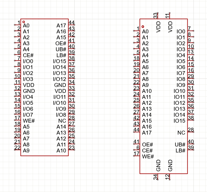
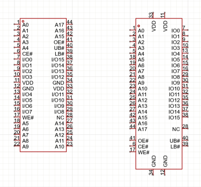 For instance, do you organize the pinout for an IC by pin number or by pin function, grouping the power pins and the ADC pins and so on? If your audience is trying to figure out the circuit logic, you should probably go functional. But if you are trying to debug a circuit, you’re often looking at the circuit diagram to figure out what a given pin does, and the pin-number layout is more appropriate.
Do you lay out the logical flow of the circuit in the schematic, or do you try to mimic the PCB layout? Again, it could depend on how your audience will be using it. If they have access to your CAD tool, and can hop back and forth seamlessly from schematic to PCB, the logical flow layout is the win. However, if they are an audience of beginners, or stuck with a PDF of the schematic, or trying to debug a non-working board, perhaps the physical layout is the right approach.
Al Williams, who has experience with projects of a much larger scale than most of us self-taught hackers, doesn’t even think that a schematic makes sense. He thinks that it’s much easier to read and write the design in a hardware description language like VHDL. Of course, that’s certainly true for IC designs, and probably also for boards of a certain complexity. But this is only true when your audience is also familiar with the HDL in question. Otherwise, you’re writing in Finnish for an audience of Spaniards.
Before this conversation, I was thinking of schematic layout as Tom Nardi described it on the podcast – a step along the way to get to the fun parts of PCB layout and then to getting the boards in hand. But at least in our open-source hardware world, it’s also a piece of the documentation, and a document that has an audience of peers who it pays to keep in mind just as much as when I’m sitting down and writing this very newsletter. In some ways, it’s the same thing.
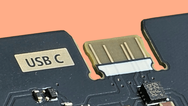
(And yeah, I know the featured image doesn’t exactly fit the topic, but I love it anyway.)