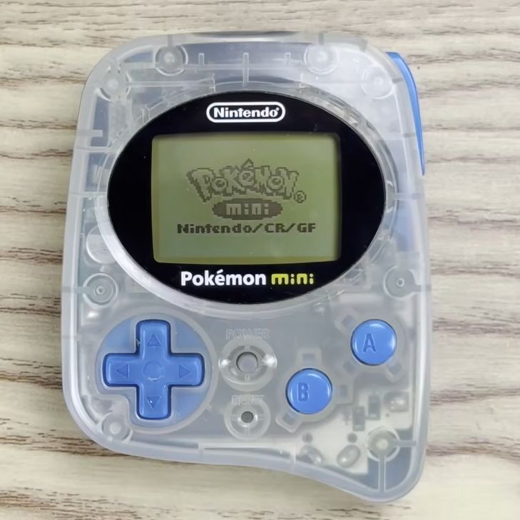
Originally only sold at the Pokémon Center New York in late 2001 for (inflation adjusted) $80, the Pokémon Mini would go on to see a release in Japan and Europe, but never had more than ten games produced for it. Rather than Game Boy-like titles, these were distinct mini games that came on similarly diminutive cartridges. These days it’s barely remembered, but it can readily be used for homebrew titles, as [Inkbox] demonstrates in a recent video.

Inside the device is an Epson-manufactured 16-bit S1C88 processor that runs at 4 MHz and handles basically everything, including video output to the monochrome 96×64 pixel display. System RAM is 4 kB of SRAM, which is enough for the basic games that it was designed for.
The little handheld system offered up some capabilities that even the full-sized Game Boy couldn’t match, such as a basic motion sensor in the form of a reed relay. There’s also 2 MB of ROM space directly addressable without banking.
Programming the device is quite straightforward, not only because of the very accessible ISA, but also the readily available documentation and toolchain. This enables development in C, but in the video assembly is used for the added challenge.
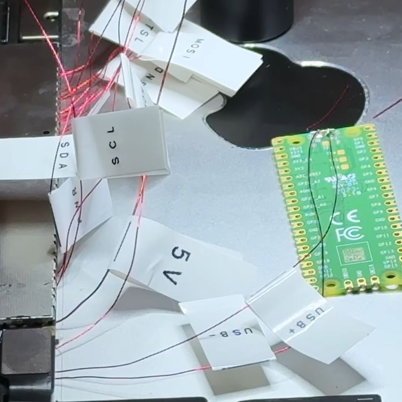
Making the screen tiles can be done in an online editor that [Inkbox] also made, and the game tested in an emulator prior to creating a custom cartridge that uses an RP2040-based board to play the game on real hardware. Although a fairly obscure gaming handheld, it seems like a delightful little system to tinker with and make more games for.
Continue reading “Exploring Homebrew For The Pokémon Mini” →