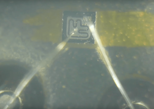
Building things in a lab is easy, at least when compared to scaling up for mass production. That’s why there are so many articles about fusion being right around the corner, or battery technology that’ll allow aviation to switch away from fossil fuels, or any number of other miraculous solutions that never come into being. They simply don’t scale or can’t be manufactured in a cost effective way. But even when they are miraculous and can be produced on a massive scale, as is the case for things like transistors, there are some oddities that come up as a result of the process of making so many. This video goes into some of the intricacies of a bipolar junction transistor (BJT) and why it looks the way it does.
The BJT in this video is a fairly standard NPN type, with three layers of silicon acting as emitter, base, and collector. Typically when learning about electronics devices the drawings of them are simplified two-dimensional block diagrams, but under a microscope this transistor at first appears nothing like the models shown in the textbook. Instead it resembles more of a bird’s foot with a few small wires attached. The bird’s foot shape is a result of attempting to lower the undesirable resistances of the device and improve its performance, and some of its other quirks are due to the manufacturing process. That process starts with a much larger layer of doped silicon that will eventually become the collector, and then the other two, much smaller, layers of the transistor deposited on top of the collector. This also explains while it looks like there are only two layers upon first glance, and also shows that the horizontal diagram used to model the device is actually positioned vertically in the real world.
For most of the processes in our daily lives, the transistor has largely been abstracted away. We don’t have to think about them in a computer that much anymore, and unless work is being done on high-wattage power electronics devices, radios, or audio amplifiers it’s not likely that an average person will run into a transistor. But this video goes a long way to explaining the basics of one of the fundamental building blocks of the modern world for those willing to take a dive into the physics. Take a look at this video as well for an intuitive explanation of the close cousin of the BJT, the field-effect transistor.
Continue reading “The Geometry Of Transistors” →


