A few years ago, writing for a blog called Motherboard of all things, [Emanuel Maiberg] wrote PC Gaming Is Still Way Too Hard. The premise is that custom building a gaming PC is too hard, because you have to source components and comparison shop. Again, this was written for Motherboard. Personally, I would have shopped that story around a bit more. Now, the same author is back again, telling us PC Building Simulator is way more fun than building a real computer. It’s my early nomination for worst tech article of the year.
Speaking of motherboards, This is a GoFundMe project to re-create the Amiga 4000 mainboard, with schematics. Building PCs is too hard, but the Amiga architecture is elegant. Some of these boards are dying due to electrolytic capacitor and battery leakage. This project is aiming to deconstruct an original A4000 board and turn it into Gerbers and schematics, allowing new boards to be manufactured. Building a PC is way too hard, but with this GoFundMe, you won’t have to design an entire system from scratch. Don’t worry, I already tipped off the Motherboard editors to this one.
Alright, story time. In 6th grade science class, the teacher was awesome. On the days when there was really no chance of any learning happening (the day before Christmas break, the last day of school), the teacher broke out the Electric Chicken. What’s an Electric Chicken? It’s a test tube rack, two wires, and a Wimshurst generator. “Here, grab ahold of this for as long as you can.” It got even cooler when you get a bunch of kids to hold hands and tell them pride is better than pain. Here’s a Kickstarter for a mini Wimshurst generator. It’s made out of PCBs! Hat tip to [WestfW] for finding this one.
It’s no secret that I get a lot of dumb press releases. Most of these are relegated to the circular file folder. It’s also no secret I get a lot of ICO announcements hitting my email. These, also, are trashed. I recently received a press release for an ICO that goes beyond anything else. ONSTELLAR is a blockchain-powered social media network for paranormal and metaphysical enthusiasts. It’s the crypto for Coast to Coast AM listeners, UFO enthusiasts, and people who think PKE meters are real. This is it, we’ve reached peak crypto.
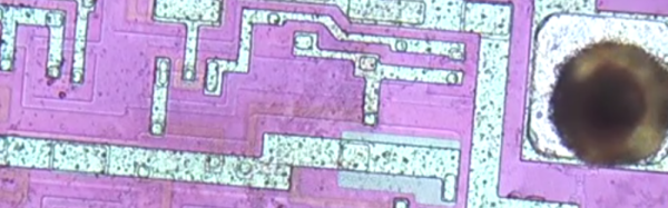
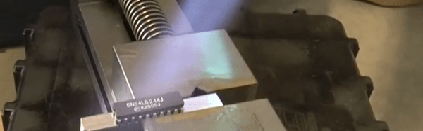
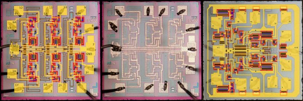
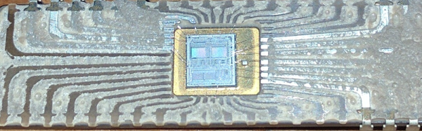
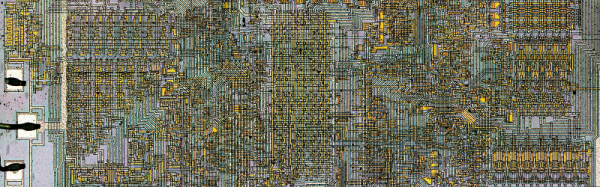
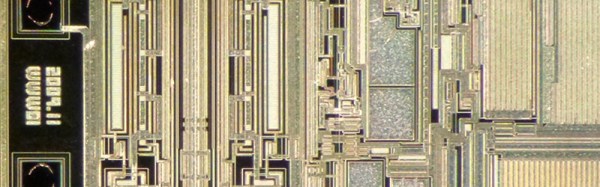
If you want to decapsulate an IC — and why wouldn’t you? — the usual way of doing things involves dropping acid, ego death, toxic chemicals, and a fume hood. There is another way. Here’s [A Menadue] decapping a quartz watch IC with just fire. The process is about as ‘hold my beer’ as you would expect. Just take a small butane torch, heat up a chip, and recover the die. A bit of ultrasonic cleaning later and you get a pretty clean chip. Microscope not included.