We know what you’re thinking: this is yet another one of those “Gut the retro gear for its cool old case and then fill it up with IoT junk” projects. Well, rest assured that extending and enhancing this 1970s computer trainer is very much an exercise in respecting the original design, and while there’s a Pi inside, it doesn’t come close to spoiling the retro goodness.
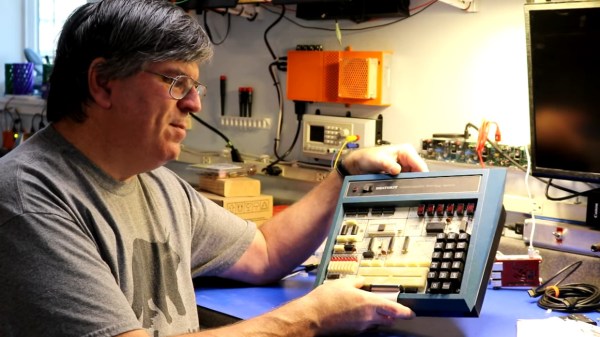
Like many of a similar vintage as [Scott M. Baker], the Heathkit catalog was perhaps only leafed through marginally less than the annual Radio Shack catalog. One particularly desirable Heathkit item was the ET-3400 microcomputer learning system, which was basically a 6800-based computer surrounded by a breadboarding area for experimentation. [Scott] got a hold of one of these, but without the optional expansion accessory that would allow it to do interesting things such as running BASIC or even supporting a serial port. So [Scott] decided to roll his own expansion board.
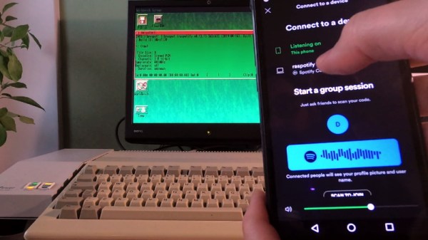
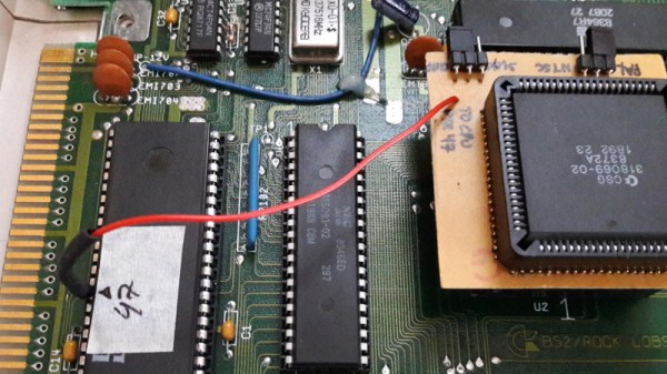
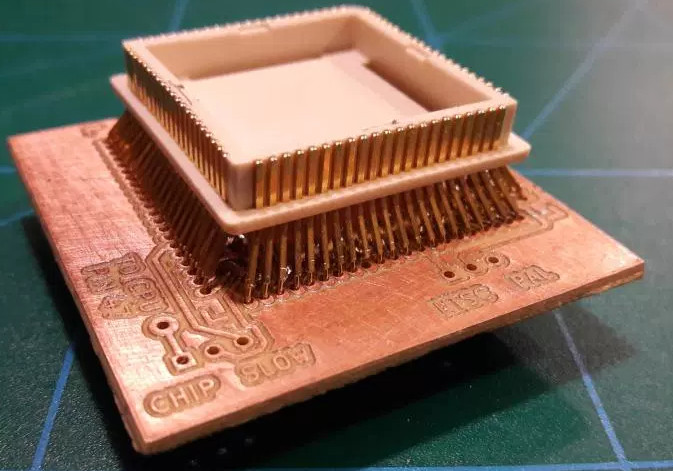
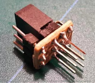
The expansion card that [Scott] designed is not strictly a faithful reproduction, at least in terms of the original BOM. He turned to more modern — and more readily available — components, but still managed to provide the serial port, cassette interface, and RAM/ROM expansion of the original unit. The Raspberry Pi is an optional add-on, which just allows him to connect wirelessly if he wants. The card fits into a 3D-printed case that sits below the ET-3400 and maintains the original trainer’s look and feel. The longish video below shows the build and gives a tour of the ET-3400, both before and after the mods.
It looks as though trainers like these and other artifacts from the early days of the PC revolution are getting quite collectible. Makes us wish we hadn’t thrown some things out.
Continue reading “Retro Computer Trainer Gets A Raspberry Pi Refit”