Ask Hackaday: What’s Your Etchant?

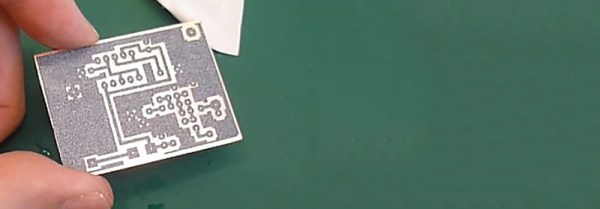
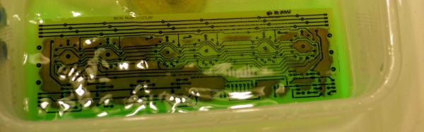
Although the typical cliché for a mad scientist usually involves Bunsen burners, beakers, and retorts, most of us (with some exceptions, of course) aren’t really chemists. However, there are some electronic endeavors that require a bit of knowledge about chemistry or related fields like metallurgy. No place is this more apparent than producing your own PCBs. Unless you use a mill, you are probably using a chemical bath of some sort to strip copper from your boards.

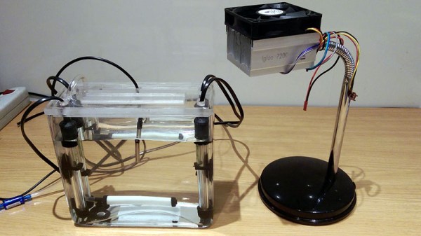
The standard go-to solution is ferric chloride. It isn’t too tricky to use, but it does work better hot and with aeration, although neither are absolutely necessary. However, it does tend to stain just about everything it touches. In liquid form, it is more expensive to ship, although you can get it in dry form. Another common etchant is ammonium or sodium persulphate.

pcby
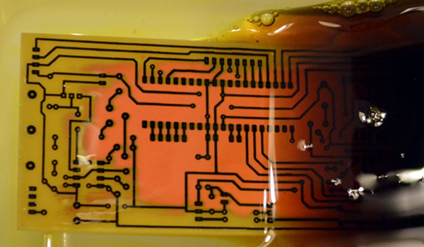
There’s also a variety of homemade etchants using things like muriatic acid and vinegar. Most of these use peroxide as an oxidizer. There’s lots of information about things like this on the Internet. However, like everything on the Internet, you can find good information and bad information.

When [w_k_fay] ran out of PCB etchant, he decided to make his own to replace it and wrote a great guide on how this is done. He found a lot of vague and conflicting information on the Internet. He read that the vinegar solution was too slow and the cupric acid needs a heated tank, a way to oxygenate the solution, and strict pH controls. However, he did have successful experiments with the hydrochloric acid and peroxide. He also used the same materials (along with some others) to make ferric chloride successfully.

Continue reading “Ask Hackaday: What’s Your Etchant?”

Vacuum Exposure Unit Gives Better PCB Etching Results

PCB etching seems to be a subject that sharply divides our community into those who are experts in it and etch themselves every PCB they use, and those who have significant quantities of ferric chloride stained clothing in their past and for whom the advent of cheap commercial PCB manufacture and CNC milled PCB prototyping have been the best thing since sliced bread.

Your likely success when etching your own boards is most dependent on the quality of your preparation and your equipment. If you began your PCB career with etch-resist transfers and a permanent marker with a Tupperware tub of etchant, then later progressed to laser toner or photographic masking and a bubble etcher, you’ll understand this.

[Jana Marie Hemsing] has drawn our attention to this very nicely built PCB etching suite (Translation, German original) at the Warpzone hackerspace (Translation, German original) in Münster, Germany. The foil pattern is printed on transparency and exposed to UV light over a photoresist coated board with a vacuum pump arrangement to ensure as good a contact as possible to the board for the sharpest result. They have two exposers, one for single sided and the other for double-sided boards, both are very well-built from what looks like plywood.

The attention to detail continues with a home-made magnetic stirrer and heated bubble etching tank Their etchant of choice is sodium persulphate, so there are none of those brown ferric chloride stains.

PCB etching is nothing new, indeed we have covered the subject extensively over the years. But we think you’ll agree, if you’re going to etch your own PCBs you should have as good a set-up as you can, and Warpzone’s PCB suite is rather well put together. Those of us in spaces with lesser facilities should be getting ideas from it.

Etching PCBs With A 3D Printer

With the coming of very cheap blue laser diodes, PCB fabrication has become increasingly interesting. Instead of making a photoresist, placing it over a piece of pre-sensitized copper clad board, and putting the whole assemblage under a blacklight, it’s possible to put a photomask on a board with a tiny bit of very blue light. All you need is a CNC machine. A 3D printer can be a very precise CNC machine, and when you combine these two ideas together, you can make printed circuit boards with an Ultimaker.

[Geggo] had the idea of attaching a blue laser diode to his Ultimaker to burn a few traces into presensitized copper board. With a 3D printed adapter, he was able to mount the diode and associated electronics right on the extruder body. With a small ring to tighten up the aperture, [geggo] was able to put a 50 micrometer wide dot of light on a piece of copper. The laser is powered directly from the PWM fan output on the printer controller board, allowing this entire mish-mash of cheap electronics to be controlled via G-code.

A few experiments were necessary to determine the correct speeds and power settings, with the best results being 1000 mm per minute at 40 mA. The finished board looks fantastic, and a few minutes after [geggo] was done etching a board, he started using his 3D printer as a printer. It’s a result that is so good, so easy to accomplish, and requires so little effort it makes us wonder why we don’t see more of this.

Even Easier Toner Transfer PCBs

One of the most popular methods of homebrew PCB fabrication is the toner transfer process. Compared to UV-sensitive films and CNC mills, the toner transfer process is fantastically simple and only requires a laser printer. Being simple doesn’t mean it’s easy, though, and successful toner transfer depends on melting the toner to transfer it from a piece of paper to a copper clad board.

This is heatless toner transfer for PCB fabrication. Instead of using a clothes iron or laminator to transfer toner from a paper to board, [simpletronic] is doing it chemically using acetone and alcohol.

Acetone usually dissolves laser printer toner, and while this is useful for transferring a PCB from paper to board, it alone is insufficient. By using a mixture of eight parts alcohol to three parts acetone, [simpletronic] can make the toner on a piece of paper stick, but not enough to dissolve the toner or make it blur.

From there, it’s a simple matter of putting a piece of paper down on copper clad board. After waiting a few minutes, the paper peels off revealing perfectly transferred board art. All the usual etching techniques can be used to remove copper and fabricate a PCB.

This is an entirely novel method of PCB fabrication, but it’s not exactly original. A few days ago, we saw a very similar method of transferring laser printed graphics to cloth, wood, and metal. While these are probably independent discoveries, it is great evidence there are still new techniques and new ways of doing things left to be discovered.

Thanks [fridgefire] for the tip.

The Ultimate Tool For Homebrew PCB Manufacturing

While OSHPark, Seeed Studio, and DirtyPCB have taken most of the fun and urgency out of making your own circuit boards at home, there are still a few niche cases and weird people who like to go it alone. For them, [Jarzębski] has created the ultimate homebrew PCB manufacturing solution (.pl, here’s the Google translatrix).

[Jarzębski] is using UV-sensitive photomasks for his PCBs, but he’s not doing something simple like a blacklight to develop his boards. He’s using a 30 Watt UV LED for exposing his boards. This, of course, generates a lot of heat and to mitigate that he’s added a Peltier cooler, temperature sensor, and a fan to cool off this retina-burning LED. 30 Watts will get the job done, considering [Jarzębski] was using a quartet of 4.5W LEDs before this build.

Developing a PCB is only one part of the equation; you need to etch it, too. For this, [Jarzębski] is using a small 1.6 Liter aquarium and four aquarium heaters for dunking 120mm x 120mm PCBs in the tank. There’s no mention of what chemistry [Jarzębski] is using – ferric chloride, cupric chloride, or otherwise – but the heaters and aerator should make etching go very smoothly.

There’s a video (English) going over the rest of the project below.

Continue reading “The Ultimate Tool For Homebrew PCB Manufacturing”

A Stack Of Boards For An Edison Breadboard Adapter

The Intel Edison is a neat piece of hardware, but the connector for the Edison is extremely intimidating and the Mini breakout board is incompatible with breadboards. What’s [Federico], a builder of Internet of Things to do? Etch their own breakout board.

The Mini Breakout board for the Intel Edison is the official ‘minimal’ offering for getting the Edison up and running with a mess of jumper wires and LEDs. While this breakout board handles the USB to UART bridge, power regulation, and exposes all the pins on the Edison connector, it is terrible for prototyping. It’s a 4×14 array of holes on a 0.1″ grid that are hidden underneath the Edison.

[Federico] handled this problem with a copper clad board and a little bit of ferric chloride. He jumped into Eagle and created a breakout board to turn the 4×14 pin grid into a more sensible breadboard-friendly layout.

The breadboard-friendly adapter doesn’t have level shifters, but by using the mini-breakout board between the Edison and the breadboard adapter [Federico] still has the UART to USB hardware and a battery charging circuit. Still, there’s room for improvement and we can’t wait to see what he comes up with next.

Toner Transfer And Packing Tape

The toner transfer process of producing PCBs has evolved tremendously over the last few years. It started out by printing PCB layouts onto magazines with a laser printer, then some clever people figured out that glossy inkjet photo paper would work just as well. Now there’s a new substrate for you – packing tape – and it seems to work pretty well.

[David] was designing a cheap board for a robot kit for a workshop and needed 100 tiny PCBs. They were simple boards, and perfectly suited for home PCB manufacturing. He started off by printing directly onto glossy magazine paper, but this wasn’t an ideal solution. During one run, some of the toner landed on the packaging tape he was using to secure the boards. A bit of serendipity came into play and [David] discovered packaging tape is usable in the toner transfer process.

The technique is simple enough: put some packaging tape on a piece of paper, print a board layout (reversed!) on a laser printer, and go through the usual clothes iron/laminator/etching process. [David] is actually using a hair straightener for transferring the toner over to the copper clad board – interesting, and in a pinch you can use the same tool for reflowing SMD components.