Interview: Mill CPU For Humans Parts 3 And 4

Welcome back to the conclusion of our interview on Mill CPU architecture with [Ivan Godard]. If you missed yesterday’s offering you can watch the preview video or go back and read the original article. Above is the third part, with the final installment found after the break.

We’d like to address some concerns from the comments of yesterday’s post. Several readers noted that Mill is only in the simulation phase. [Ivan] is very up-front about that… there is no silicon. But that doesn’t mean we should disregard a company that looks to build on successes from the current generation of processors while avoiding their drawbacks. It is incredibly costly to design silicon from scratch. This is why we don’t see new architectures sprouting up on a monthly basis.

We simply think it’s exciting to see what kinds of changes may be coming and how designers plan to accomplish advances in processing power while reducing power consumption at the same time.

Continue reading “Interview: Mill CPU For Humans Parts 3 And 4”

Interview: New Mill CPU Architecture Explanation For Humans

Hackaday had an amazing opportunity to sit down with [Ivan Godard] who discussed the Mill CPU development which his company — Out of the Box Computing —  has been working on for about a decade. The driving force behind Mill development is that optimizations to existing architectures can only get you so far. At some point you need to come up with a new processor that builds on success and failure of its predecessors.

Ivan’s team has put out several lecture videos linked from their site that dig really deep into the inner workings that give Mill an advantage over currently available chips. We covered one of them recently which prompted [Ivan] to reach out to us. But what if you aren’t working on your advanced degree in semiconductor design? Our interview certainly isn’t for the laymen, but any engineering enthusiast should find this a refreshing and delightful conversation. After the jump you can see the first two installments of the four part interview.

Continue reading “Interview: New Mill CPU Architecture Explanation For Humans”

The Mill CPU Architecture

There are basically two ways to compute data. The first is with a DSP, a chip that performs very specialized functions on a limited set of data. These are very cheap, have amazing performance per watt, but can’t do general computation at all. If you’d like to build a general-purpose computer, you’ll have to go with a superscalar processor – an x86, PowerPC, or any one of the other really beefy CPU architectures out there. Superscalars are great for general purpose computing, but their performance per watt dollar is abysmal in comparison to a DSP.

A lot of people have looked into this problem and have come up with nothing. This may change, though, if [Ivan Godard] of Out-of-the-Box computing is able to produce The Mill – a ground-up rethink of current CPU architectures.

Unlike DSPs, superscalar processors you’d find in your desktop have an enormous amount of registers, and most of these are rename registers, or places where the CPU stores a value temporarily. Combine this with the fact that connecting hundreds of these temporary registers to places where they’ll eventually be used eats up about half the power budget in a CPU, and you’ll see why DSPs are so much more efficient than the x86 sitting in your laptop.

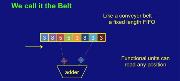
[Ivan]’s solution to this problem is replacing the registers in a CPU with something called a ‘belt’ – basically a weird combination of a stack and a shift register. The CPU can take data from any position on the belt, perform an operation, and places the result at the front of the belt. Any data that isn’t used simply falls off the belt; this isn’t a problem, as most data used in a CPU is used only once.

On paper, it’s a vastly more efficient means of general purpose computation. Unfortunately, [Ivan] doesn’t quite have all the patents in for The Mill, so his talks (two available below) are a little compartmentalized. Still, it’s one of the coolest advances in computer architecture in recent memory and something we’d love to see become a real product.

Continue reading “The Mill CPU Architecture”

The Nintendo Switch CPU Exposed

Ever wonder what’s inside a Nintendo Switch? Well, the chip is an Nvidia Tegra X1. However, if you peel back a layer, there are four ARM CPU cores inside — specifically Cortex A57 cores, which take up about two square millimeters of space on the die. The whole cluster, including some cache memory, takes up just over 13 square millimeters. [ClamChowder] takes us inside the Cortex A57 inside the Nintendo Switch in a recent post.

Interestingly, the X1 also has four A53 cores, which are more power efficient, but according to the post, Nintendo doesn’t use them. The 4 GB of DRAM is LPDDR4 memory with a theoretical bandwidth of 25.6 GB/s.

The post details the out-of-order execution and branch prediction used to improve performance. We can’t help but marvel that in our lifetime, we’ve seen computers go from giant, expensive machines to the point where a game console has 8 CPU cores and advanced things like out-of-order execution. Still, [ClamChowder] makes the point that the Switch’s processor is anemic by today’s standards, and can’t even compare with an outdated desktop CPU.

Want to program the ARM in assembly language? We can help you get started. You can even do it on a breadboard, though the LPC1114 is a pretty far cry from what even the Switch is packing under the hood.

Clockhands For Faster CPU Execution

When you design your first homebrew CPU, you probably are happy if it works and you don’t worry as much about performance. But, eventually, you’ll start trying to think about how to make things run faster. For a single CPU, the standard strategy is to execute multiple instructions at the same time. This is feasible because you can do different parts of the instructions at the same time. But like most solutions, this one comes with a new set of problems. Japanese researchers are proposing a novel way to work around some of those problems in a recent paper about a technique they call Clockhands.

Suppose you have a set of instructions like this:

LOAD A, 10
LOAD B, 20
SUB A,B
LOAD B, 30
JMPZ  DONE
INC B

If you do these one at a time, you have no problem. But if you try to execute them all together, there are a variety of problems. First, the subtract has to wait for A and B to have the proper values in them. Also, the INC B may or may not execute, and unless we know the values of A and B ahead of time (which, of course, we do here), we can’t tell until run time. But the biggest problem is the subtract has to use B before B contains 30, and the increment has to use it afterward. If everything is running together, it can be hard to keep straight.

Continue reading “Clockhands For Faster CPU Execution”

The 13.5 Million Core Computer

Having a dual- or quad-core CPU is not very exotic these days and CPUs with 12 or even 16 cores aren’t that rare. The Andromeda from Cerebras is a supercomputer with 13.5 million cores. The company claims it is one of the largest AI supercomputers ever built (but not the largest) and can perform 120 Petaflops of “dense compute.”

We aren’t sure about the methodology, but they also claim more than one exaflop of “AI computing.” The computer has a fabric backplane that can handle 96.8 terabits per second between nodes. According to a post on Extreme Tech, the core technology is a 3-plane wafer processor, WSE-2. One plane is for communications, one holds 40 GB of static RAM, and the math plane has 850,000 independent cores and 3.4 million floating point units.

The data is sent to the cores and collected by a bank of 64-core AMD EPYC 3 processors. Andromeda is optimized to handle sparse matrix computations. The company claims that the performance scales “almost linearly.” That is, as you double the number of cores used, you roughly half the total run time.

The machine is available for remote use and cost about $35 million to build. Since it uses 500 kW at peak run times, it isn’t free to operate, either. Extreme Tech notes that the Frontier computer at Oak Ridge National Labs is both larger and more precise, but it cost $600 million, so you’d expect it to be more capable.

Most homebrew “supercomputers” we see are more for learning how to work with clusters than trying to hit this sort of performance. Of course, if you have a modern graphics card, OpenCL and CUDA will let you do some of this, too, but at a much lesser scale.

Tesla’s Dojo Is An Interesting CPU Design

What do you get when you cross a modern super-scalar out-of-order CPU core with more traditional microcontroller aspects such as no virtual memory, no memory cache, and no DDR or PCIe controllers? You get the Tesla Dojo, which Chips and Cheese recently did a deep dive on.

It starts with a comparison to the IBM Cell processors. The Cell of the mid-2000s featured something called the SPE (Synergistic Processing Elements). They were smaller cores focused on vector processing or other specialized types of workloads. They didn’t access the main memory and had to be given tasks by the fully featured CPU. Dojo has 1.25MB of SRAM that it can use as working memory with five ports, but it has no cache or virtual memory. It uses DMA to get the information it needs via a mesh system. The front end pulls RISC-V-like (heavily MIPS-inspired) instructions into a small instruction cache and decodes eight instructions per cycle. Continue reading “Tesla’s Dojo Is An Interesting CPU Design”