Last time, I showed you a simple PWM block and an open source UART core. This time, I’ll put these parts together to create a PC PWM output peripheral.
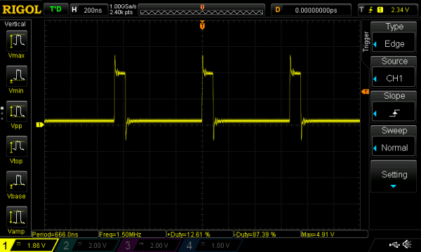
Last time, I showed you a simple PWM block and an open source UART core. This time, I’ll put these parts together to create a PC PWM output peripheral.
We’ve done a lot of posts on how to use the Lattice iCEstick ranging from FPGA tutorials to how to use one as a logic analyzer. If you picked up one of these inexpensive boards here’s a fun little experiment. [T4D10N] saw a project [Hamster] put together to send SOS on the FM radio band using nothing but an FPGA. [Hamster used a Spartan], so he decided to do the same trick using an iCEstick with the open source IceStorm tools.
You might be surprised that the whole thing only takes 53 lines of Verilog — less if you cut out comments and whitespace. That’s because it uses the FPGA’s built-in PLL to generate a fast clock and then uses a phase accumulator divider to produce three frequencies on the FM radio band; one for a carrier and two for a tone, spaced 150 Hz apart. The result is really frequency shift keying but you can hear the results on an FM radio.
Continue reading “ICEstick Makes Terrible Radio Transmitter”
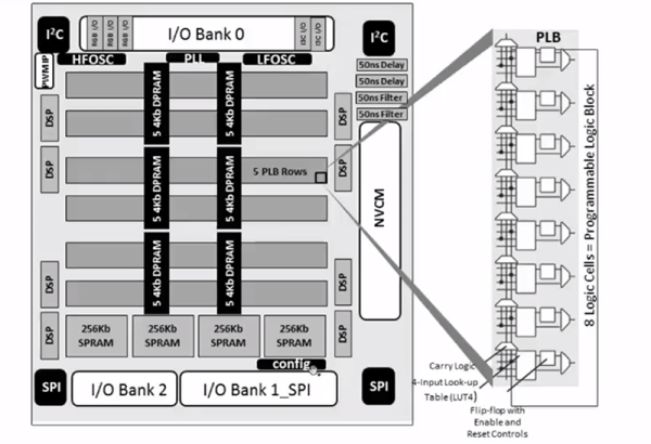
It is no secret that we like the Lattice iCE40 FPGA. It has a cheap development board and an open source toolchain, so it is an easy way to get started developing low-cost, low-power FPGA designs. There are a few members of the family that have similar characteristics including the top-of-the-line UltraPlus. [Steve] from Lattice and [Michael Klopfer] from the University of California Irvine have a three-part video series that explain the architecture of the devices. Altogether, the videos are about an hour long and — of course — they use the official tools, not IceStorm. But it is still a great time investment if you have an iCE40 board and you want to understand what the chip has under the hood.
The first part is fairly short and talks a lot about applications. There’s also a nod to the hobbyist use of FPGAs. Keep in mind that the iCE40 FPGAs come in different sizes and variants, so don’t get excited when you see them mention a RISC-V — that isn’t going to fit in your iCEStick, that we know of. The iCEstick has a HX-1K onboard, which is the high-performance variant with 1,280 logic elements, as opposed to the low-power (LP) version.
Continue reading “Three Part Deep Dive Explains Lattice ICE40 FPGA Details”
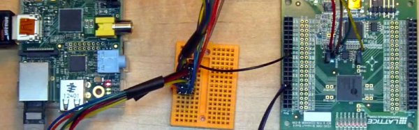
The Linux kernel recently added support for loading firmware into an FPGA via the FPGA Manager Framework. [OpenTechLab] has built a driver for the Lattice iCE40 FPGA (same chip used on the iCEStick and other development boards). One attraction to the iCE40 is there is an open source toolchain called iCEStorm.
Even if you aren’t specifically interested in FPGAs, the discussion about Linux device drivers is good background. The principles would apply to other drivers, and would definitely apply if you want to write another FPGA loader.
Continue reading “Lattice ICE40 FPGA Configured By Linux Kernel”
Unlike microcontroller projects, projects involving FPGAs cannot yet claim to rely on a mature open-source toolchain. Each FPGA will, at some point, need to be configured with a proprietary bitstream produced from a closed source synthesis tool. This lack of a full FPGA toolchain to take your project from Verilog-or-VHDL to an uploadable bitstream is due to many reasons. First, writing such a “compiler” is complicated. It involves intimate knowledge of the resources available on the FPGA that can assimilate the functionality of the intended design. Second, the entire synthesis procedure is closed-source, a “secret sauce” of sorts for each FPGA vendor.
In response, [Alex] and [Clifford] have taken the first step towards an open-source toolchain for one FPGA; they’ve reverse-engineered the bitstream of Latttice Semiconductor’s iCE40 FPGA. The duo didn’t just pick the iCE40 on a whim. This choice was deliberately because that FPGA is available on a development board for a mere $22 so that others could follow in their footsteps without breaking the bank.
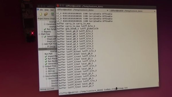
In the video below, [Clifford] demos the functionality of this new tool by synthesizing a design from Verilog to a bitstream and then back from a bitstream to Verilog. Given this feature, a staggering amount of work has been done towards developing a polished open-source toolchain for this particular FGPA.
To snag a copy of the latest code, have a look at its documentation page.
Continue reading “Reverse Engineering Lattice’s ICE40 FPGA Bitstream”
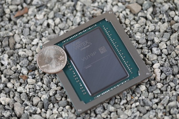
Xilinx recently announced the Virtex UltraScale+ VU19P FPGA. Of course, FPGA companies announce new chips every day. The reason this one caught our attention is the size of it: nearly 9 million logic cells and 35 billion transistors on a chip! If that’s not enough there is also over 2,000 user I/Os including transceivers that can move around 4.5 Tb/s back and forth.
To put things in perspective, the previous record holder — the Virtex Ultrascale 440 — has 5.5 million logic cells and an old-fashioned Spartan 3 topped out at about 50,000 cells — the new chip has about 180 times that capacity. For the record, I’ve built entire 32-bit CPUs on smaller Spartans.
That led us to wonder? Who’s buying these things? When I first heard about it I guessed that the price would be astronomical, partly due to expense but also partly because the market for these has to be pretty small. The previous biggest Xilinx part is listed on DigKey who pegs the Ultrascale 440 (an XCVU440-2FLGA2892E) at a cost of $55,000 as a non-stocked item. Remember, that chip has just over half the logic cells of the VU19P.
Continue reading “Who Could Possibly Need An FPGA With 9M Logic Cells And 35B Transistors?”

Sometimes you start something simple and then it just leads to a chain reaction of things. I wanted to write a post about doing state machines in Verilog and target the Lattice iCEstick board that we often use for quick FPGA projects. That led to a small problem: how do you show what’s going on inside? In this series of posts, we’ll look at building a logic analyzer into an FPGA to help debug itself, instantiating memory, and — finally — state machines.
Logic analysis is a common tool in FPGA development. If you use Altera, they have Signal Tap available that lets you build a simple logic analyzer into the FPGA that talks back to your PC. Xilinx has ChipScope which is about the same. Sometimes those tools either cost money or are limited in some way in the free versions. I have my sights set on a tool that can be used with the Lattice architecture.
Sure, you can ship data out on I/O pins and then use a regular logic analyzer to pick up the data. But that isn’t very handy. So I thought about writing a generic logic analyzer component. But before I did I decided to check to see if someone else had already done it.
Spoiler alert: they did, but I wanted something a little different so I wound up extending the program significantly. What I wound up with is a reasonably portable Verilog logic analyzer that can produce traces like this one:
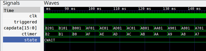
Keep in mind, this isn’t a simulation. This is real data pulled off the actual FPGA. Yes, that is gtkwave producing the plots, but the input data is a VCD file generated from samples taken inside the FPGA.
Continue reading “Logic Analyzers For FPGAs: A Verilog Odyssey”