Computers can write poetry, even if they can’t necessarily write good poetry. The same can be said of routing PC boards. Computers can do it, but can they do it well? Of course, there are multiple tools each with pluses and minuses. However, a slick web page recently announced deeppcb.ai — a cloud-based AI router — and although details are sparse, there are a few interesting things about the product.
First, it supports KiCAD. You provide a DSN file, and within 24 hours you get a routed SES file. Maybe. You get three or four free boards –apparently each week — after which there is some undisclosed fee. Should you just want to try it out, create an account (which is quick and free — just verify your e-mail and create a password). Then in the “Your Boards” section there are a few examples already worked out.
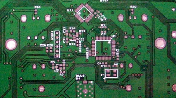
When designing a printed circuit board, there are certain rules. You should place decoupling capacitors near the power pins to each chip. Your ground planes should be one gigantic fill of copper; two ground planes connected by a single trace is better known as an antenna. Analog sections should be kept separate from digital sections, and if you’re dealing with high voltage, that section needs to be isolated.
One that I hear a lot is that you must never put a 90-degree angle on a trace. Some fear the mere sight of a 90-degree angle on a PCB tells everyone you don’t know what you’re doing. But is there is really no greater sin than a 90-degree trace on a circuit board?
This conventional wisdom of eschewing 90-degree traces is baked into everything we know about circuit board design. It is the first thing you’re taught, and it’s the first thing you’ll criticize when you find a board with 90-degree traces. Do square traces actually matter? The short answer is no, but there’s still a reason we don’t do it.
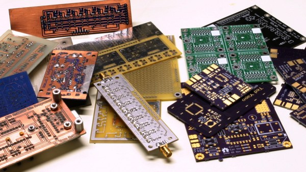
Many readers are certainly familiar with the process for home-etching of PCBs: it’s considered very straightforward, if a little involved, today. This was not the case in my youth, when I first acquired an interest in electronics. At that time, etching even single-sided boards was for “advanced” hobbyists. By the time I started etching my own PCBs, the advanced hobbyists were on to double-sided home-etched boards — the only type not pictured above, because I couldn’t find the one successful example I ever created. I later saw the rise of “bare bones” fabricated PCBs: professionally made fixed size boards with plated-through holes, but no soldermask or silkscreen. Eventually, this gave way to the aggregating PCB services we have now with full two-layer boards, complete with soldermask and silkscreen.
Today, the “advanced” hobbyist may be using four-layer boards, although the four-layer adoption rate is still relatively low – OSH Park produces around 90% two-layer and 10% four-layer, for instance. I think this will inevitably increase, as has been the case with all the previous technologies: the advanced eventually becomes the mainstream. Each of the previous shifts has brought easier design and construction as well as improved performance, and the same will be true as four layers becomes more commonplace.
When current flows through a conductor it becomes an inductor, when there is an inductor there is an electromagnetic field (EM). This can cause a variety of issues during PCB layout if you don’t plan properly, and sometimes we get burned even when we think we have planned for unwanted inductance and the effects that come with them.
When doing high speed logic we need to be able to deliver sudden changes in current to the devices if we want to have proper switching times and logic levels. Unfortunately inductance is usually not a friend in these circumstances as it resists those sudden changes in current. If the high speed devices are driving capacitive loads, which themselves are resisting changes in voltage, even more instantaneous current is needed.
Simply put, inductors resist a change of current, and can act as a low pass filter when in series with the signal or power supply flow. Inductors do this by storing energy in the flux surrounding the conductor. Alternatively capacitors resist a change in voltage (again by storing energy) and can act as a high pass filter when in series with the signal. This makes them a valuable tool in the fight against unwanted inductance in power supply distribution.
In the video below, and the remainder of this article, I’m going to dive into the concept of inductance and how it affects our design choices when laying out circuit boards.
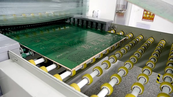
The availability of low-cost, insanely high-quality PCBs has really changed how we do electronics. Here at Hackaday we see people ditching home fabrication with increasing frequency, and going to small-run fab for their prototypes and projects. Today you can get a look at the types of factory processes that make that possible. [Scotty Allen] just published a (sponsored) tour of a PCB fab house that shows off the incredible machine tools and chemical baths that are never pondered by the world’s electronics consumers. If you have an appreciation PCBs, it’s a joy to follow a design through the process so take your coffee break and let this video roll.
Several parts of this will be very familiar. The photo-resist and etching process for 2-layer boards is more or less the same as it would be in your own workshop. Of course the panels are much larger than you’d ever try at home, and they’re not using a food storage container and homemade etchant. In fact the processes are by and large automated which makes sense considering the volume a factory like this is churning through. Even moving stacks of boards around the factory is show with automated trolleys.
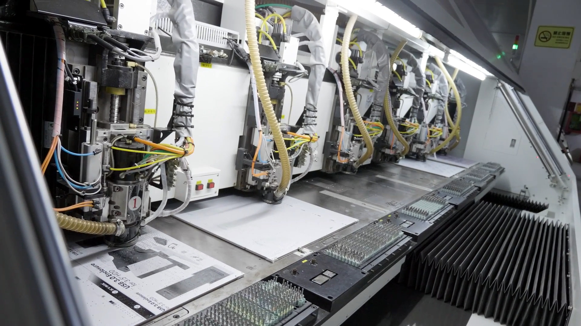
Six headed PCB drilling machine (four heads in use here).
What we find most interesting about this tour is the multi-layer board process, the drilling machines, and the solder mask application. For boards that use more than two layers, the designs are built from the inside out, adding substrate and copper foil layers as they go. It’s neat to watch but we’re still left wondering how the inner layers are aligned with the outer. If you have insight on this please sound off in the comments below.
The drilling process isn’t so much a surprise as it is a marvel to see huge machines with six drill heads working on multiple boards at one time. It sure beats a Dremel drill press. The solder mask process is one that we don’t often see shown off. The ink for the mask is applied to the entire board and baked just to make it tacky. A photo process is then utilized which works much in the same way photoresist works for copper etching. Transparent film with patterns printed on it cures the solder mask that should stay, while the rest is washed away in the next step.
Boards continue through the process to get silk screen, surface treatment, and routing to separate individual boards from panels. Electrical testing is performed and the candy making PCB fab process is complete. From start to finish, seeing the consistency and speed of each step is very satisfying.
Just about anyone can make a simple LED cube. But what if you want to make a 1-meter cube using 512 LEDs? [Hari] wanted to do it, so he created two different kinds of LED boards using EasyEDA. There are 270 of each type of board, for a total of 540 (there are only 512 LEDs, so we guess he got some spares due to how the small boards panelized). The goal is to combine these boards to form a cube measuring over three feet on each side.
To simplify wiring, the boards are made to daisy chain like a cordwood module. However, to get things to line up, each column of LED boards have to rotate 90 degrees. You can see several videos about the project below.
[Helentronica] has been using Altium Designer to lay out PC boards since he was a student. Now as a freelancer, he felt like he didn’t quite know all that he wanted to know. Keep in mind he’d done multilayer boards with BGAs and LVDS routing, so he was no neophyte. He decided to spend about $200 on an advanced course from Fedevel Academy. In this day where everything is free on the Internet, is it worth paying $200 to watch some videos?
[Helentronica] probably weighed the same question. However, he was interested in the course project which is an open-source computer module with an i.MX6 processor, 1 GB of DDR3 SDRAM and lots of expansion options. In fact, the ad copy that sold him was:
You will be practicing on a real high-speed board with 1.2GHz CPU and DDR3, PCIE, SATA, HDMI, LVDS, 1Gb Ethernet and more
He completed the course. Was it worth it? We won’t spoil the story, but you should check out his post and find out. Even if you don’t want to drop $200 or you don’t use Altium, you will probably pick up some tips on PC board layout.