What Every PCB Designer Needs To Know About Track Impedance With Eric Bogatin

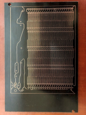
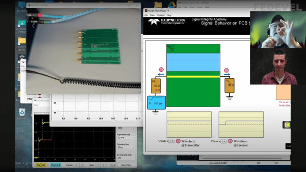
PCB design starts off being a relatively easy affair — you create a rectangular outline, assign some component footprints, run some traces, and dump out some Gerber files to send to the fab. Then as you get more experienced and begin trying harder circuits, dipping into switching power supplies, high speed digital and low noise analog, things get progressively more difficult; and we haven’t even talked about RF or microwave design yet, where things can get just plain weird from the uninitiated viewpoint. [Robert Feranec] is no stranger to such matters, and he’s teamed up with one of leading experts (and one of this scribe’s personal electronics heroes) in signal integrity matters, [Prof. Eric Bogatin] for a deep dive into the how and why of controlled impedance design.

RG58 cable construction. These usually are found in 50 Ω and less commonly these days 75Ω variants

One interesting part of the discussion is why is 50 Ω so prevalent? The answer is firstly historical. Back in the 1930s, coaxial cables needed for radio applications, were designed to minimize transmission loss, using reasonable dimensions and polyethylene insulation, the impedance came out at 50 Ω. Secondarily, when designing PCB traces for a reasonable cost fab, there is a trade-off between power consumption and noise immunity.

As a rule of thumb, lowering the impedance increases noise immunity at the cost of more power consumption, and higher impedance goes the other way. You need to balance this with the resulting trace widths, separation and overall routing density you can tolerate.

Another fun story was when Intel were designing a high speed bus for graphical interfaces, and created a simulation of a typical bus structure and parameterized the physical constants, such as the trace line widths, dielectric thickness, via sizes and so on, that were viable with low-cost PCB fab houses. Then, using a Monte Carlo simulation to run 400,000 simulations, they located the sweet spot. Since the via design compatible with the cheap fab design rules resulted often in a via characteristic impedance that came out quite low, it was recommended to reduce the trace impedance from 100 Ω to 85 Ω differential, rather than try tweak the via geometry to bring it up to match the trace. Fun stuff!

We admit, the video is from the start of the year and very long, but for such important basic concepts in high speed digital design, we think it’s well worth your time. We certainly picked up a couple of useful titbits!

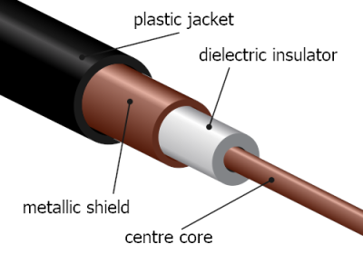
Now we’ve got the PCB construction nailed, why circle back and go check those cables?

Continue reading “What Every PCB Designer Needs To Know About Track Impedance With Eric Bogatin”

PCB Thermal Design Hack Chat

Join us on Wednesday, March 30 at noon Pacific for the PCB Thermal Design Hack Chat with Mike Jouppi!

Most of the time, designing a printed circuit board is a little like one of those problems in an introductory physics course, the ones where you can safely ignore things like air resistance. With PCBs, it’s generally safe to ignore things like trace heating and other thermal considerations in favor of just getting everything placed sensibly and routing all the traces neatly.

But eventually, the laws of physics catch up to you, and you’ll come across a real-world problem where you can’t just hand-wave thermal considerations aside. When that happens, you’ll want to have a really good idea of just how much a trace is going to heat up, and what it’s going to do to the performance of your board, or even if the PCB is going to survive the ordeal.

join-hack-chatDigging into the thermal properties of PCBs is something that Mike Jouppi has been doing for years. After working in the aircraft industry as a mechanical engineer, he started Thermal Management LLC, which developed software to make the thermal design of PCBs easier. He’ll stop by the Hack Chat to answer your questions about PCB thermal design considerations, and help us keep all our hard work from going up in smoke.

Our Hack Chats are live community events in the Hackaday.io Hack Chat group messaging. This week we’ll be sitting down on Wednesday, March 30 at 12:00 PM Pacific time. If time zones have you tied up, we have a handy time zone converter.
Continue reading “PCB Thermal Design Hack Chat”

The Benefits Of Critiquing Your Own PCB Designs

In a recent retrospective video, [Phil] from Phil’s Lab goes through a number of his early PCB designs, to critique and comment on what he likes and doesn’t like in these designs. Even though it’s only been a few a few years, he founds plenty that’s wrong. From poor and inconsistent formatting in the schematic, to sloppy and outright broken PCB layouts. It’s a fascinating look at years of lessons learned.

[Phil] comments on the importance of clear labeling and organization of sections and pages in the schematic to make it obvious what the function of a block is. Other lessons include the labeling of nets to make PCB routing a lot easier, making good use of PCB planes, getting all relevant information on components and layout in the schematic as a comment, and connecting decoupling capacitors to their relevant pins.

Although we tend to forget about older projects, it can be very interesting to take a look at them now and then, to see (hopefully) our progress over the years. In the case of [Phil] it’s fascinating to see the transition from a basic two-sided board with THT components to multi-layer boards with STM32 MCUs.

Continue reading “The Benefits Of Critiquing Your Own PCB Designs”

JavaScript App Uses Advanced Math To Make PCBs Easier To Etch

We all remember the litany from various math classes we’ve taken, where frustration at a failure to understand a difficult concept bubbles over into the classic, “When am I ever going to need to know this in real life?” But as we all know, even the most esoteric mathematical concepts have applications in the real world, and failure to master them can come back to haunt you.

Take Voronoi diagrams, for example. While we don’t recall being exposed to these in any math class, it turns out that they can be quite useful in a seemingly unrelated area: converting PCB designs into easy-to-etch tessellated patterns. Voronoi diagrams are in effect a plane divided into different regions, or “cells”, each centered on a “seed” object. Each cell is the set of points that are closer to a particular seed than they are to any other seed. For PCBs the seeds can be represented by the traces; dividing the plane up into cells around those traces results in a tessellated pattern that’s easily etched.

To make this useful to PCB creators, [Craig Iannello] came up with a JavaScript application that takes an image of a PCB, tessellates the traces, and spits out G-code suitable for a laser engraver. A blank PCB covered with a layer of spray paint, the tessellated pattern is engraved into the paint, and the board is etched and drilled in the usual fashion. [Craig]’s program makes allowances for adding specific features to the board, like odd-shaped pads or traces that need specific routing.

This isn’t the first time we’ve seen Voronoi diagrams employed for PCB design, but the method looks so easy that we’d love to give it a try. It even looks as though it might work for CNC milling of boards too.

Modular Vibrating ‘Bots Made From PCBs

Printed circuit boards, they’re a medium designed primarily to mount electrical components with the wires themselves places as copper traces on the boards. To accommodate wide range of needs that have arisen over decades, board houses have evolved all manner of advanced techniques in routing and plating. To our benefit, this also makes it possible to leverage PCBs in an entirely artistic way, taking advantage of the highly-optimized manufacturing process. [GeeekClub] did just that, creating awesome vibrating robots out of custom-made PCBs.

The ‘bots come as a single PCB, with the parts snapped out akin to removing parts from sprues in a plastic model kit. They can then be assembled, with a pair of pager vibration motors installed to provide motive power. But really it’s the aesthetic of the boards and not the functionality that make these so incredible.

The design nestles a coin cell in the base of each bot, providing power and using the weight to help keep them upright. There’s a smattering of LEDs on board, and the art style of the ‘bots draws from Hopi Indian, Asian, and South American influences.

Cyphercon 2017 featured these exciting cubic badges, created from PCBs and soldered by hand.
This Star Trek inspired piece shows just how far you can go with the right color soldermask and some creativity.

This “flat-pack” style of PCB design that comes to life with creative use of angles and layers is becoming its own sub-genre of the art. The Star Trek Enterprise inspired build in another great example. We’ve also seen a growing trend of using the PCB as enclosures, take the Cyphercon badge and Queercon badge projects from 2017 as examples. Get yourself up to speed on design techniques for using FR4 as an enclosure from [Voja Antonic’s] in-depth guide.

Transform Kicad Design To Patchwork For Isolation Routing

Tuning a desktop router and your board designs for isolation routing can be a bit tricky, with thin traces usually being the first victim. For simple prototype boards you usually don’t need tightly packed traces, you just want to isolate the nets. To do this with a minimum amount of routing, [Michael Schembri] created kicad-laser-min, a command-line utility that takes a Kicad PCB design and expands all the tracks and pads to their maximum possible width.

Laser scribed PCB with maximum track widths

The software takes one layer of the PCB layout, converts it to black and white, and then runs a C++ Voronoi algorithm on it to dilate each track and pad until it meets another expanding region. Each region is colourised, and OpenCV edge detection is used to produce the contours that need to be milled or etched. A contour following algorithm is then used to create the G-code. The header image shows the output of each step.

Full source code is available on GitHub. [Michael] has had good results with his own boards, which are scribed using a laser cutter before etching, but welcomes testing and feedback from other users. He has found that OpenCV doesn’t always completely close all the contours, but the gaps are usually smaller than the engraving width of his laser, so no shorts are created.

This is basically “Scribble style” prototyping with CAD and CNC tools. If you prefer scribe and etch, you might consider building a simple PCB shaker for faster etching. If you have a router but want to avoid the dust, you can use a carbide scribe to scratch out the tracks without needing to etch.

DeepPCB Routes Your KiCAD PCBs

Computers can write poetry, even if they can’t necessarily write good poetry. The same can be said of routing PC boards. Computers can do it, but can they do it well? Of course, there are multiple tools each with pluses and minuses. However, a slick web page recently announced deeppcb.ai — a cloud-based AI router — and although details are sparse, there are a few interesting things about the product.

First, it supports KiCAD. You provide a DSN file, and within 24 hours you get a routed SES file. Maybe. You get three or four free boards –apparently each week — after which there is some undisclosed fee. Should you just want to try it out, create an account (which is quick and free — just verify your e-mail and create a password). Then in the “Your Boards” section there are a few examples already worked out.

Continue reading “DeepPCB Routes Your KiCAD PCBs”