Swapping Vinyl For Cardboard With This ESP32 Turntable

Cardboard is a surprisingly durable material, especially in its corrugated form. It’s extremely lightweight for its strength, is easy to work, can be folded and formed into almost any shape, is incredibly inexpensive, and when it has done its duty it can be recycled back into more paper. For these reasons, it’s often used in packaging material but it can be used to build all kinds of things outside of ensuring that products arrive at their locations safely. This working cardboard record player is one example.

While the turntable doesn’t have working records in the sense that the music is etched into them like vinyl, each has its own RFID chip embedded that allows the ESP32 in the turntable’s body to identify them. Each record corresponds to a song stored on an SD card that instructs the ESP32 to play the appropriate song. It also takes care of spinning the record itself with a small stepper motor. There are a few other details on this build that tie it together too, including a movable needle arm held on with a magnet and a volume slider.

As far as a building material goes, cardboard is fairly underrated in our opinion. Besides small projects like this turntable, we’ve also seen it work as the foundation for a computer, and it even has the strength and durability to be built into a wall or even used as shelving material. And, of course, it’s a great material to use when prototyping new designs.

Continue reading “Swapping Vinyl For Cardboard With This ESP32 Turntable”

Apple May Use Electrical Debonding For Battery Replacement

As a result of the European Union’s push for greater repairability of consumer devices like smartphones, Apple sees itself forced to make the batteries in the iPhone user-replaceable by 2027. Reportedly, this has led Apple to look at using electroadhesion rather than conventional adhesives which require either heat, isopropyl alcohol, violence, or all of the above to release. Although details are scarce, it seems that the general idea would be that the battery is wrapped in metal, which, together with the inside of the metal case, would allow for the creation of a cationic/anionic pair capable of permanent adhesion with the application of a low-voltage DC current.

This is not an entirely wild idea. Tesa has already commercialized it in the electrical debonding form of its Debonding on Demand product. This uses a tape that’s applied to one side of the (metal) surfaces, with a 5 bar pressure being applied for 5 seconds. Afterwards, the two parts can be released again without residue as shown in the above image. This involves applying a 12V DC voltage for 60 seconds, with the two parts afterward removable without force.

Continue reading “Apple May Use Electrical Debonding For Battery Replacement”

Long-Term OctoPrint Stat Manipulation Uncovered

Developing free and open source software can be a thankless experience. Most folks do it because it’s something they’re passionate about, with the only personal benefit being the knowledge that there are individuals out there who found your work useful enough to download and install. So imagine how you’d feel if it turns out somebody was playing around with the figures, and the steady growth in the number of installs you thought your software had turned out to be fake.

That’s what happened just a few days ago to OctoPrint developer [Gina Häußge]. Although there’s no question that her software for remotely controlling and monitoring 3D printers is immensely popular within the community, the fact remains that the numbers she’s been using to help quantify that popularity have been tampered with by an outside party. She’s pissed, and has every right to be.

Continue reading “Long-Term OctoPrint Stat Manipulation Uncovered”

This Week In Security: Kaspersky Ban, Project Naptime, And More

The hot news this week is that Kaspersky is banned in the USA. More specifically, Kaspersky products will be banned from sale in the US starting on September 29. This ban will extend to blocking software updates, though it’s unclear how that will actually be accomplished. It’s reasonable to assume that payment processors will block payments to Kaspersky, but will ISPs be required to block traffic that could contain antivirus updates?

WordPress Plugin Backdoor

A Quartet of WordPress plugins have been found to have recently included backdoor code. It’s a collection of five Open Source plugins, seemingly developed by unrelated people. Malicious updates first showed up on June 21st, and it appears that all five plugins are shipping the same malicious code.

Rabbit AI API

The Rabbit R1 was released to less than thunderous applause. The idea is a personal AI device, but the execution has been disappointing, to the point of reviewers suggesting some of the earlier claims were fabricated. Now it seems there’s a serious security issue, in the form of exposed API keys that have *way* too many privileges.

The research seems to be done by the rabbitude group, who found the keys back in May. Of the things allowed by access to the API keys, the most worrying for user privacy was access to every text-to-speech call. Rabbitude states in their June 25 post, that “rabbit inc has known that we have had their elevenlabs (tts) api key for a month, but they have taken no action to rotate the api keys.” On the other hand, rabbit pushed a statement on the 26th, claiming they were just then made aware of the issue, and made the needed key rotations right away.

Continue reading “This Week In Security: Kaspersky Ban, Project Naptime, And More”

FLOSS Weekly Episode 789: You Can’t Eat The Boards

This week Jonathan Bennett and Doc Searls chat with Igor Pecovnik and Ricardo Pardini about Armbian, the Debian-based distro tailor made for single-board computers. There’s more than just Raspberry Pi to talk about, with the crew griping about ancient vendor kernels, the less-than-easy ARM boot process, and more!

Continue reading “FLOSS Weekly Episode 789: You Can’t Eat The Boards”

Paul Allen’s Living Computers Museum And Labs To Be Auctioned

After the Living Computers museum in Seattle closed like so many museums and businesses in 2020 with the pandemic, there were many who feared that it might not open again. Four years later this fear has become reality, as the Living Computers: Museum + Labs (LCM+L, for short) entire inventory is being auctioned off. This occurs only 12 years after the museum and associated educational facilities were opened to the public. Along with Allen’s collection at the LCM+L, other items that he had been collecting until his death in 2018 will also be auctioned at Christie’s, for a grand total of 150 items in the Gen One: Innovations from the Paul G. Allen Collection.

In 2022 Allen’s art collection had seen the auction block, but this time it would seem that the hammer has come for this museum. Unique about LCM+L was that it featured vintage computing systems that visitors could interact with and use much like they would have been used back in the day, rather than being merely static display pieces, hence the ‘living computers’ part. Although other vintage computing museums in the US and elsewhere now also allow for such interactive displays, it’s sad to see the only major vintage computing museum in Washington State vanish.

Hopefully the items being auctioned will find loving homes, ideally at other museums and with collectors who aren’t afraid to keep the educational spirit of LCM+L alive.

Thanks to [adistuder] for the tip.

Top image: A roughly 180° panorama of the “conditioned” room of the Living Computer Museum, Seattle, Washington, USA. Taken in 2014. (Credit: Joe Mabel)

TSMC’s Long Path From Round To Square Silicon Wafers

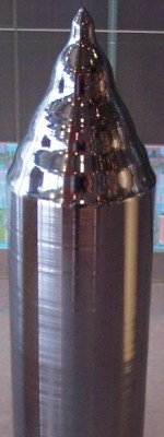
Crystal of Czochralski-grown silicon.

Most of us will probably have seen semiconductor wafers as they trundle their way through a chip factory, and some of us may have wondered about why they are round. This roundness is an obvious problem when one considers that the chip dies themselves are rectangular, meaning that a significant amount of the dies etched into the wafers end up being incomplete and thus as waste, especially with (expensive) large dies. This is not a notion which has escaped the attention of chip manufacturers like TSMC, with this particular manufacturer apparently currently studying a way to make square substrates a reality.

According to the information provided to Nikkei Asia by people with direct knowledge, currently 510 mm x 515 mm substrates are being trialed which would replace the current standard 12″ (300 mm) round wafers. For massive dies such as NVidia’s H200 (814 mm2), this means that approximately three times as many would fit per wafer. As for when this technology will go into production is unknown, but there exists significant incentive in the current market to make it work.

As for why wafers are round, this is because of how these silicon wafers are produced, using the Czochralski method, named after Polish scientist [Jan Czochralski] who invented the method in 1915. This method results in rod-shaped crystals which are then sliced up into the round wafers we all know and love. Going square is thus not inherently impossible, but it will require updating every step of the process and the manufacturing line to work with this different shape.