There’s a lot of little things that can go wrong before you get great results out of a process. We like to read build logs to learn from the mistakes made. [Marc Liyanage] bought a Nomad CNC machine from Carbide3d, and after a bit of learning has gotten some very nice PCBs out of it.
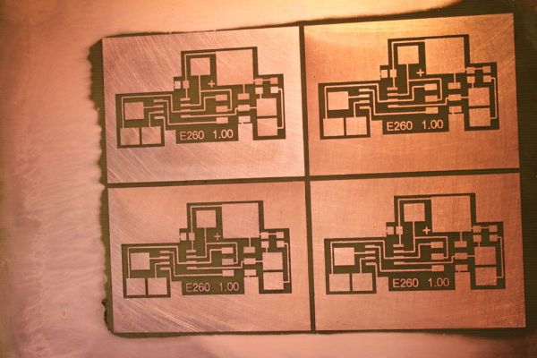
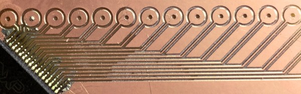
The first trip up he encountered was not setting the design rules in EagleCAD to check for gaps too small for his router bit. After he sorted that, and worked around an issue with Carbide not supporting R values for curves; instead opting for IJK, he made a nice TQFP to DIP break out board.
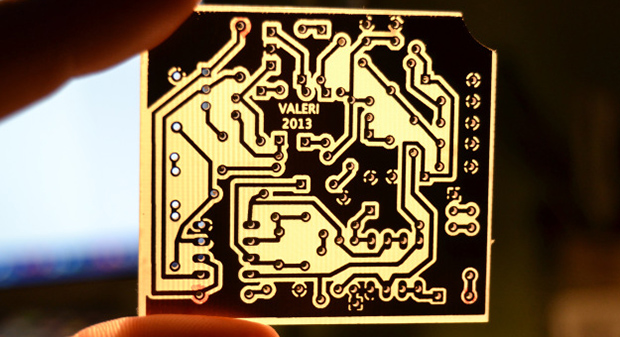
The next board was a more complicated double-sided job. He cleverly had the machine drill two holes all the way through the PCB to give him a space for two alignment pins. Unfortunately this didn’t work out exactly as planned and he had a slight misalignment with some of the via holes. It looked alright and he began assembling. To his dismay, the clearances were off again. It was a bit of deja vu for us.
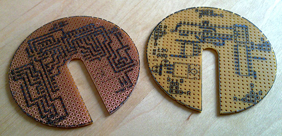
We’ve made lots of boards on a CNC machine, and can attest to the task’s finicky nature. It’s certainly quicker than the photoresist technique for boards with lots of little holes. It will take someone quite a few tries before they start having more successes than failures, but it’s very rewarding.