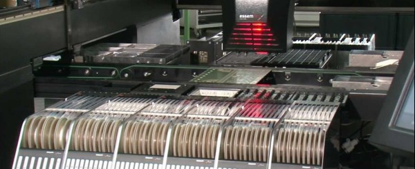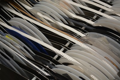
Most electronics we deal with day to day are comprised of circuit boards. No surprise there, right? But how do they work? This might seem like a simple question but we’ve all been in the place where those weird green or black sheets are little slices of magic. [Teddy Tablante] at Branch Eduction put together a lovingly crafted walkthrough flythrough video of how PCB(A)s work that’s definitely worth your time. 
[Teddy]’s video focuses on unraveling the mysteries of the PCBA by peeling back the layers of a smartphone. Starting from the full assembly he separates components from circuit board and descends from there, highlighting the manufacturing methods and purpose behind what you see.
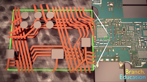
What really stands out here is the animation; at each step [Teddy] has modeled the relevant components and rendered them on the PCBA in 3D. Instead of relying solely on hard to understand blurry X-ray images and 2D scans of PCBAs he illustrates their relationships in space, an especially important element in understanding what’s going on underneath the solder mask. Even if you think you know it all we bet there’s a pearl of knowledge to discover; this writer learned that VIA is an acronym!
If you don’t like clicking links you can find the video embedded after the break. Credit to friend of the Hackaday [Mike Harrison] for acting as the best recommendation algorithm and finding this gem.
Continue reading “Journey Through The Inner Workings Of A PCB”
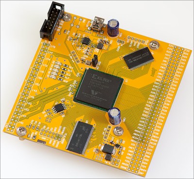 The project [Andy] had in mind for these chips was a generic dev board, which meant breaking out the IO pins and connecting some SRAM, SDRAM, and Flash memory. The first issue with this project is escape routing all the balls. Xilinx published a handy application note that recommends specific design parameters for the traces of copper under the chip. Unfortunately, this was a six-layer board, and the design rules in the application note were for 5/5mil traces. [Andy]’s board house can’t do six-layer boards, and their design rules are for 6/6mil traces. To solve this problem, [Andy] just didn’t route the inner balls, and hoped the 5mil traces would work out.