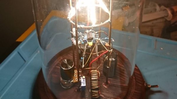
Some projects end up being more objet d’art than objet d’utile, and we’re fine with that — hacks can be beautiful too. Some hacks manage both, though, like this study in silicon and gallium under glass that serves as a bright and beautiful desk lamp.
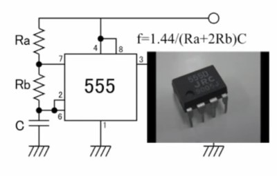
There’s no accounting for taste, of course, but we really like the way [commanderkull]’s LED filament lamp turned out, and it’s obvious that a fair amount of work went into it. Five COB filament strips were suspended from a lacy frame made of wire, which also supports the custom boost converter needed to raise the 12-volt input to the 60 volts needed by the filaments. The boost converter is based on the venerable 555 timer chip, which sits in the middle of the frame suspended by its splayed-out legs and support components. The wooden base sports a few big electrolytics and some hand-wound toroidal inductors, as well as the pot for adjusting the lamp’s brightness. The whole thing sits under a glass bell jar, which catches the light from the filaments and plays with it in a most appealing way.
There’s just something about that dead bug building technique that we love. We’ve seen it before — this potentially dangerous single-tube Nixie clock comes to mind — but we’d love to see it done more.
[via r/electronics]


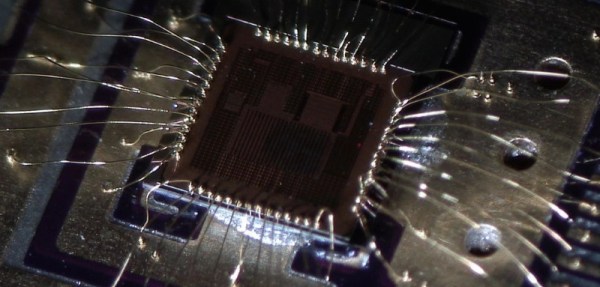
 I guess you might have a couple of lingering questions. First you’ll likely bemoan your lack of your own fabrication facility (I’m still eyeing those used 1 micron fab lines that crop up on eBay from time to time). And secondly you might be asking yourself… why?
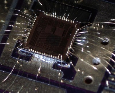