It could happen to anyone of us: suddenly you got this inkling of an idea for a product that you think might just be pretty useful or even cool. Some of us then go on to develop a prototype and manage to get enough seed funding to begin the long and arduous journey to turn a sloppy prototype into a sleek, mass-produced product. This is basically the story of how the Fitbit came to be, with a pretty in-depth article by [Tekla S. Perry] in IEEE Spectrum covering the development process and the countless lessons learned along the way.
Of note was that this idea for an accelerometer-based activity tracker was not new in 2006, as a range of products already existed, from 1960s mechanical pedometers to 1990s medical sensors and the shoe-based Nike+ step tracker that used Apple’s iPod with a receiver. Where this idea for the Fitbit was new was that it’d target a wide audience with a small, convenient (and affordable) device. That also set them up for a major nightmare as the two inventors were plunged into the wonderfully terrifying world of industrial design and hardware development.
One thing that helped a lot was outsourcing what they could to skilled people and having solid seed funding. This left just many hardware decisions to make it as small as possible, as well as waterproof and low-power. The use of the ANT protocol instead of Bluetooth saved a lot of battery, but meant a base station was needed to connect to a PC. Making things waterproof required ultrasonic welding, but lack of antenna testing meant that a closed case had a massively reduced signal strength until a foam shim added some space. The external reset pin on the Fitbit for the base station had a low voltage on it all the time, which led to corrosion issues, and so on.
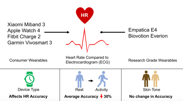
While much of this was standard development and testing fun, the real challenge was in interpreting the data from the accelerometer. After all, what does a footstep look like to an accelerometer, and when is it just a pothole while travelling by car? Developing a good algorithm here took gathering a lot of real-world data using prototype hardware, which needed tweaking when later Fitbits moved from being clipped-on to being worn on the wrist. These days Fitbit is hardly the only game in town for fitness trackers, but you can definitely blame them for laying much of the groundwork for the countless options today.
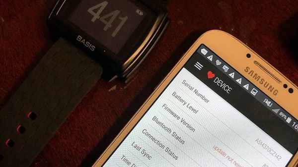
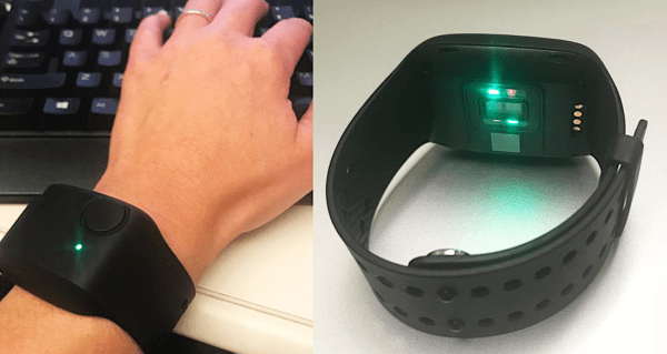
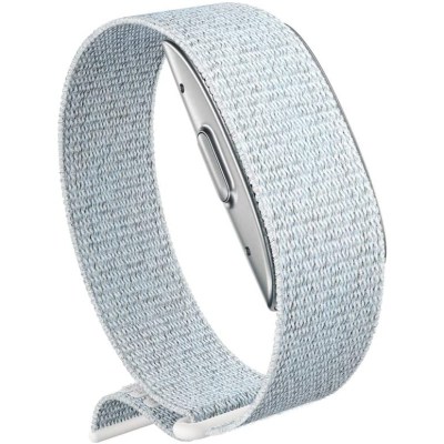 We won’t delve much in to the pros and cons of the device, other than mention two features which have the potential to creep out most folks. The device has a pair of microphones, which listen to the “tone” of your voice and report on your emotional state. The other is its use of your phone via the companion app, to take photos of you, preferably dressed in your undergarments. Your front, back and side photos get uploaded to Amazon servers, get converted to a 3D model, and then downloaded back to your phone. Amazon mentions that the photos are never retained and deleted from their servers once your 3D model is transferred back to the phone. Amazon’s ML algorithms then calculate your body fat percentage. More worryingly, the app offers a slider which you can move to see how you will “look” if you have higher or lower body fat percentages.
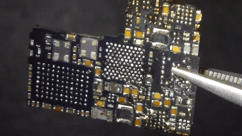
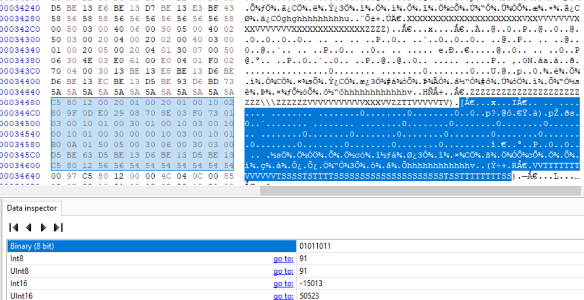
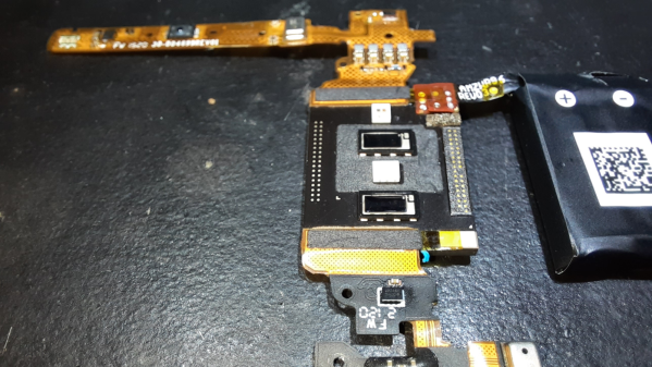
 His plan was to identify as many parts as he could, but he wasn’t very successful, and managed to identify just a few — the two MEMS microphones, two temperature sensors and the LED driver on the flex PCB, and the photo-diodes, 6-axis IMU, battery charger and flash memory on the main board. The board has an uncommon 5-layer stack up, with the centre layer being ground. PCB de-layering is a time consuming process and requires a lot of patience, but in the end, he was able to get a pretty good result. He found some oddities in the track layout and was able to identify some of the more common connections to the I2C bus and between the micro-controller and its memory. He also located several test points which seem promising for a second round of investigations. Sometime in the future, he plans to get another Halo and have a go at it using the JTAGulator and GoodFET.
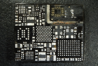