Sometime back, we announced start of a new project under the “Developed on Hackaday” series – a Badge for the Hackaday community. At its core, this badge is a single node in an Internet of Badges. At every event this badge is deployed at, a Hackaday Sub-Etha mesh network will be created, and each badge will be able to transmit and receive messages from other badge wearers. There are plans for an Sub-Etha to Internet gateway, so even if badge wearers are on the other side of the world, they’re still connected through the HaDge network.
Things have been moving along quickly, so I thought of doing a quick round-up and share progress with the community. First off, it has a name. HaDge, as in HackaDay Badge. Our objectives up until now were to set up a team, name the project, set up repositories and lock down on a working bill of materials. Within a few weeks, we’ve got all of that tied down. The HaDge group chat channel has been super active, and everyone’s been pitching in with ideas and suggestions. A spreadsheet seemed like a good idea – it let everyone add in their suggestions regarding candidate parts, create a feature list and then talk about it on the channel.
We realized early on that building the hardware is going to take some time. So in the interim, we need a dev kit platform to get in to the hands of the software developers so they can start working on the smarts that will power the HaDge. [Michele Perla] had already built JACK (Just another Cortex kit) – a development kit powered by the Atmel SAM D21. It’s pretty bare bone with just the bare minimum of parts to make it work while keeping an eye on reliability. The microcontroller+radio on the HaDge is the Atmel SAM R21 – a close relative of the D21, so it made sense to respin the JACK and create HACK (Hackaday Cortex kit) – a development kit powered by the Atmel SAM R21 that is going to be used as the core of the HaDge. [Michele] has worked hard single-handedly to complete the design and it is now ready to go for PCB fabrication soon. We are just awaiting some feedback and review of the Antenna part of the design. None of us on the hardware team have a strong RF-fu so we don’t want to make an avoidable mistake. If you’d like to review and help vet the HACK design, grab the design files from the github repo and let us know.
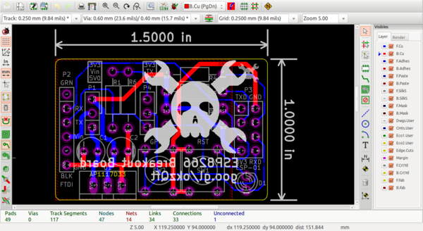
Once HACK board layout is cleared for fabrication, we’ll work on building kits that can be sent out to the software folks. We will also be working on porting the HACK design in to KiCad and this is something I have already stared work on. I started by using the neat Eagle2KiCad conversion tool by [LachlanA]. It’s not perfect, but it does reduce the work involved in porting over from Eagle to Kicad. Once that is done, hardware development for the actual HaDge will see some progress – keep a watch on the project page.


