A fun part of retro computing is saving ‘e-waste’ that was headed for certain destruction. These boards can have any number of defects, modifications and more that have to be remedied prior to using them. In the case of the Asus P5A-B Socket 7 mainboard that [Bits und Bolts] rescued from the scrapheap at least one issue was obvious: someone had ripped off the plastic part of the ZIF socket, leaving only the metal pins poking out like an awkward kind of LGA socket.
In addition to the busted PGA ZIF socket there was additional damage, including a broken SMT capacitor and missing resistor. Interestingly, someone had apparently modded the ATX power connector to permanently power on the system by removing a pin and bridging to the power-on signal. Obviously this mod had to be undone by removing the bridge and installing a new pin. After this cracked solder joints had to be addressed, before the tedious task of removing the stray PGA socket pins one by one started.
Exactly what was done to this mainboard and why will likely forever remain a mystery, but at least there didn’t seem to be any serious damage. After installing a CPU it was possible to boot and access the BIOS as well as run a couple of tools, confirming that one more Socket 7 board has been saved from the scrapper.
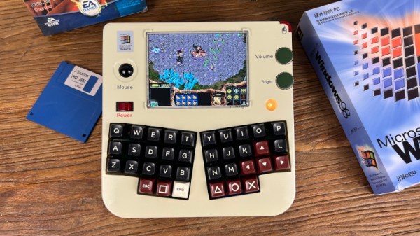
Handheld computers have become very much part of the hardware hacker scene, as the advent of single board computers long on processor power but short on power consumption has given us the tools we need to build them ourselves. Handheld retrocomputers face something of an uphill struggle though, as many of the components are over-sized, and use a lot of power. [Changliang Li] has taken on the task though, putting an industrial Pentium PC in a rather well-designed SLA printed case.
Aside from the motherboard there’s a VGA screen, a CompactFlash card attached to the IDE interface, and a Logitech trackball. As far as we can see the power comes from a USB-C PD board, and there’s a split mechanical keyboard on the top side. It runs Windows 98, and a selection of peak ’90s games are brought out to demonstrate.
We like this project for its beautiful case and effective use of parts, but we’re curious whether instead of the Pentium board it might have been worth finding a later industrial PC to give it a greater breadth of possibilities, there being few x86 SBCs. Either way it would have blown our minds back in ’98, and we can see it’s a ton of fun today. Take a look at the machine in the video below the break.
Anyone into retro Macintosh machines has probably heard of BlueSCSI: an RP2040-based adapter that lets solid state flash memory sit on the SCSI bus and pretend to contain hard drives. You might have seen it on an Amiga or an Atari as well, but what about a PC? Once upon a time, higher end PCs did use SCSI, and [TME Retro] happened to have one such. Not a fan of spinning platters of rust, he takes us through using BlueSCSI with a big-blue-based-box.
Naturally if you wish to replicate this, you should check the BlueSCSI docs to see if the SCSI controller in your PC is on their supported hardware list; otherwise, your life is going to be a lot more difficult than what is depicted on [TME Retro]. As is, it’s pretty much the same drop-in experience anyone who has used BlueSCSI on a vintage Macintosh might expect. Since the retro-PC world might not be as familiar with that, [TME Retro] gives a great step-by-step, showing how to set up hard disk image files and an iso to emulate a SCSI CD drive on the SD card that goes into the BlueSCSIv2.
This may not be news to some of you, but as the title of this video suggests, not everyone knows that BlueSCSI works with PCs now, even if it has been in the docs for a while. Of course PCs owners are more likely to be replacing an IDE drive; if you’d rather use a true SSD on that bus, we’ve got you covered.
Some time ago, Linus Torvalds made a throwaway comment that sent ripples through the Linux world. Was it perhaps time to abandon support for the now-ancient Intel 486? Developers had already abandoned the 386 in 2012, and Torvalds openly mused if the time was right to make further cuts for the benefit of modernity.
It would take three long years, but that eventuality finally came to pass. As of version 6.15, the Linux kernel will no longer support chips running the 80486 architecture, along with a gaggle of early “586” chips as well. It’s all down to some housekeeping and precise technical changes that will make the new code inoperable with the machines of the past.
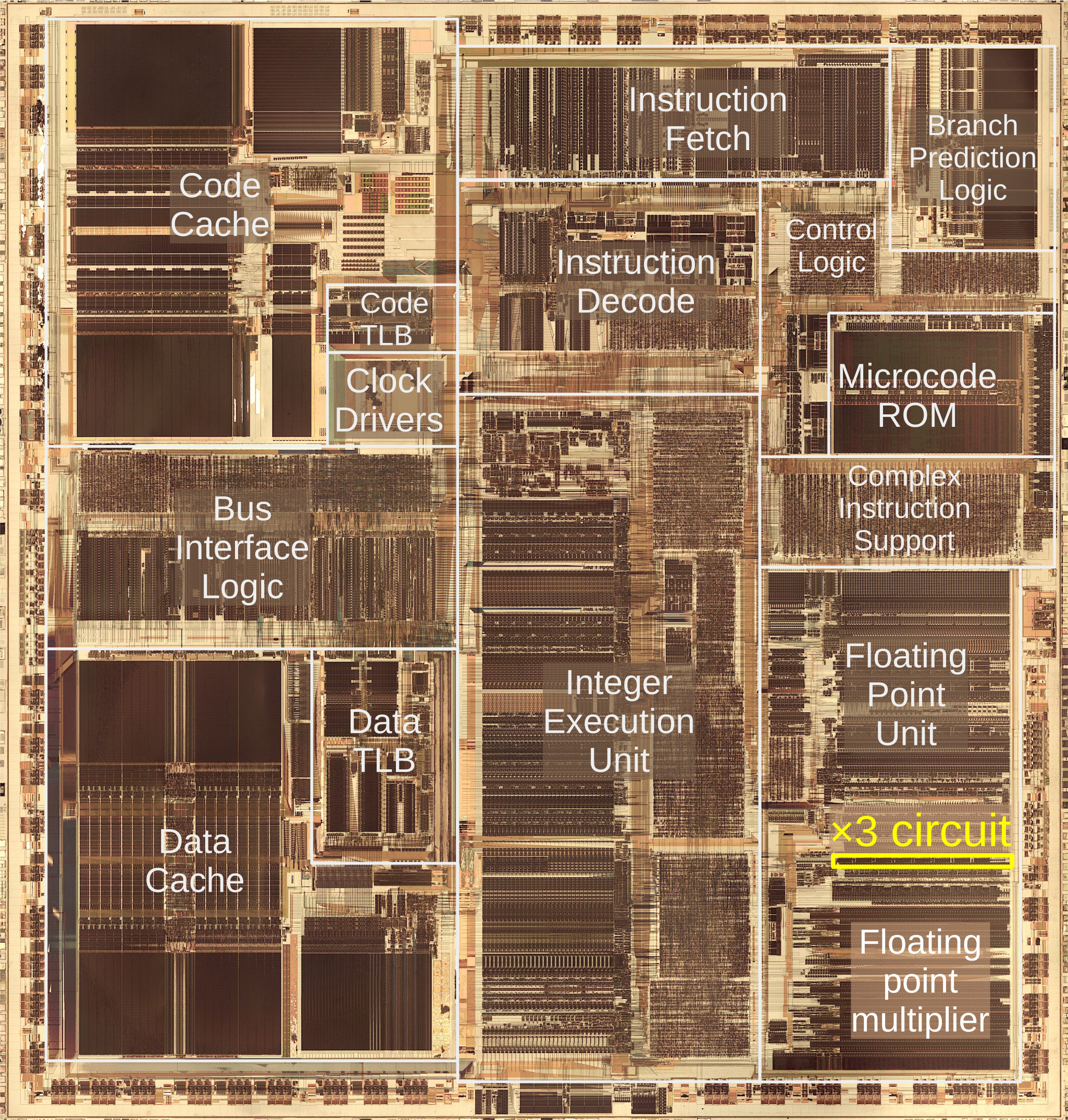
[Ken Shirriff] has been sharing a really low-level look at Intel’s Pentium (1993) processor. The Pentium’s architecture was highly innovative in many ways, and one of [Ken]’s most recent discoveries is that it contains a complex circuit — containing around 9,000 transistors — whose sole purpose is to multiply specifically by three. Why does such an apparently simple operation require such a complex circuit? And why this particular operation, and not something else?
Let’s back up a little to put this all into context. One of the feathers in the Pentium’s cap was its Floating Point Unit (FPU) which was capable of much faster floating point operations than any of its predecessors. [Ken] dove into reverse-engineering the FPU earlier this year and a close-up look at the Pentium’s silicon die shows that the FPU occupies a significant chunk of it. Of the FPU, nearly half is dedicated to performing multiplications and a comparatively small but quite significant section of that is specifically for multiplying a number by three. [Ken] calls it the x3 circuit.
The “x3 circuit”, a nontrivial portion of the Pentium processor, is dedicated to multiplying a number by exactly three and contains more transistors than an entire Z80 microprocessor.
Why does the multiplier section of the FPU in the Pentium processor have such specialized (and complex) functionality for such an apparently simple operation? It comes down to how the Pentium multiplies numbers.
Multiplying two 64-bit numbers is done in base-8 (octal), which ultimately requires fewer operations than doing so in base-2 (binary). Instead of handling each bit separately (as in binary multiplication), three bits of the multiplier get handled at a time, requiring fewer shifts and additions overall. But the downside is that multiplying by three must be handled as a special case.
[Ken] gives an excellent explanation of exactly how all that works (which is also an explanation of the radix-8 Booth’s algorithm) but it boils down to this: there are numerous shortcuts for multiplying numbers (multiplying by two is the same as shifting left by 1 bit, for example) but multiplying by three is the only one that doesn’t have a tidy shortcut. In addition, because the result of multiplying by three is involved in numerous other shortcuts (x5 is really x8 minus x3 for example) it must also be done very quickly to avoid dragging down those other operations. Straightforward binary multiplication is too slow. Hence the reason for giving it so much dedicated attention.
[Ken] goes into considerable detail on how exactly this is done, and it involves carry lookaheads as a key element to saving time. He also points out that this specific piece of functionality used more transistors than an entire Z80 microprocessor. And if that is not a wild enough idea for you, then how about the fact that the Z80 has a new OS available?
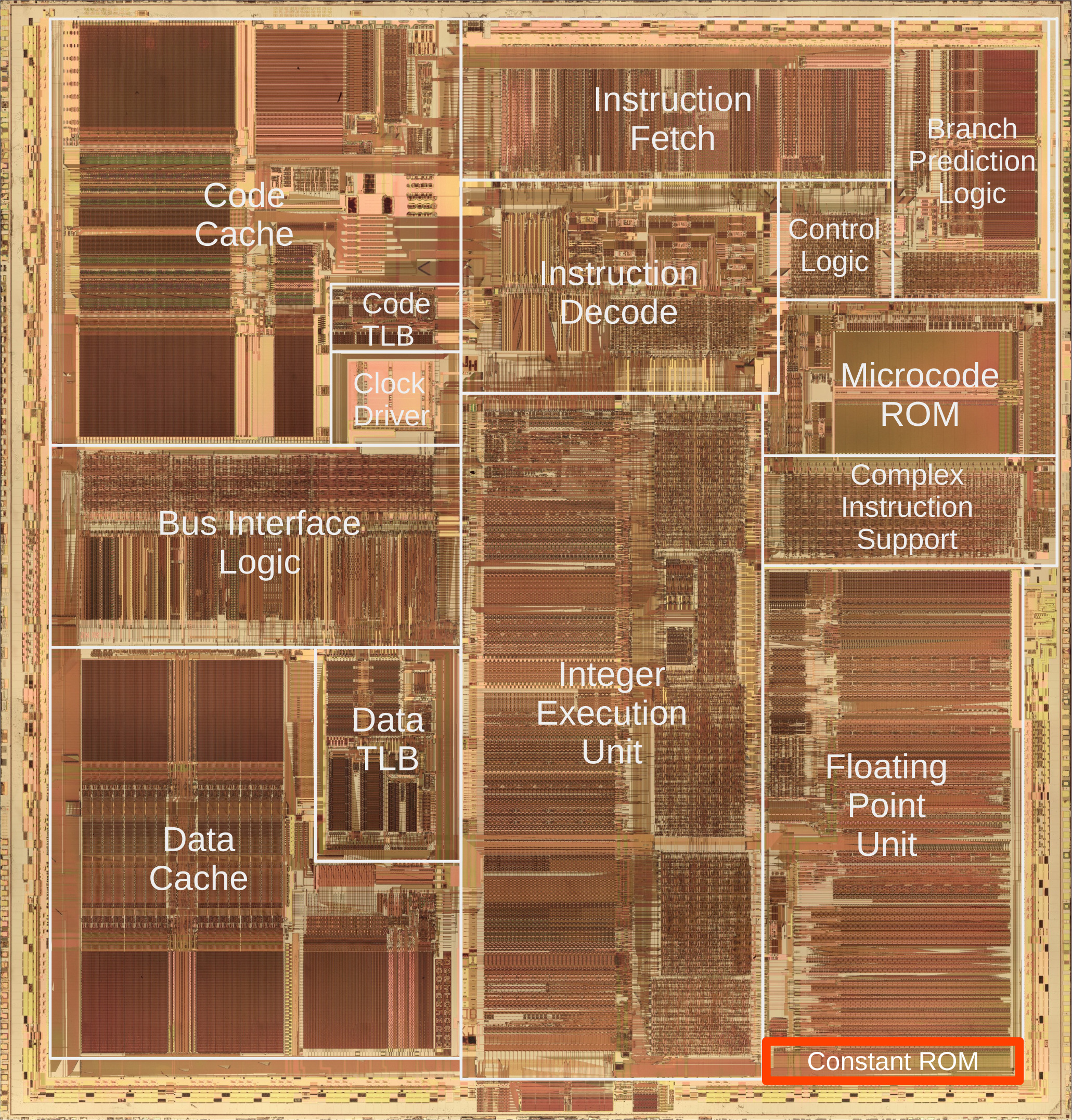
Die photo of the Intel Pentium processor with the floating point constant ROM highlighted in red. (Credit: Ken Shirriff)
Released in 1993, Intel’s Pentium processor was a marvel of technological progress. Its floating point unit (FPU) was a big improvement over its predecessors that still used the venerable CORDIC algorithm. In a recent blog post [Ken Shirriff] takes an up-close look at the FPU and associated ROMs in the Pentium die that enable its use of polynomials. Even with 3.1 million transistors, the Pentium die is still on a large enough process node that it can be readily analyzed with an optical microscope.
In the blog post, [Ken] shows how you can see the constants in each ROM section, with each bit set as either a transistor (‘1’) or no transistor (‘0’), making read-out very easy. The example looks at the constant of pi, which the Pentium’s FPU has stored as a version with no fewer than 67 significand bits along with its exponent.
The early 1990s were an interesting time in the PC world, mainly because PCs were entering the zeitgeist for the first time. This was fueled in part by companies like Intel and AMD going head-to-head in the marketplace with massive ad campaigns to build brand recognition; remember “Intel Inside”?
In 1993, Intel was making some headway in that regard. The splashy launch of their new Pentium chip in 1993 was a huge event. Unfortunately an esoteric bug in the floating-point division module came to the public’s attention. [Ken Shirriff]’s excellent account of that kerfuffle goes into great detail about the discovery of the bug. The issue was discovered by [Dr. Thomas R. Nicely] as he searched for prime numbers. It’s a bit of an understatement to say this bug created a mess for Intel. The really interesting stuff is how the so-called FDIV bug, named after the floating-point division instruction affected, was actually executed in silicon.
We won’t presume to explain it better than [Professor Ken] does, but the gist is that floating-point division in the Pentium relied on a lookup table implemented in a programmable logic array on the chip. The bug was caused by five missing table entries, and [Ken] was able to find the corresponding PLA defects on a decapped Pentium. What’s more, his analysis suggests that Intel’s characterization of the bug as a transcription error is a bit misleading; the pattern of the missing entries in the lookup table is more consistent with a mathematical error in the program that generated the table.
The Pentium bug was a big deal at the time, and in some ways a master class on how not to handle a complex technical problem. To be fair, this was the first time something like this had happened on a global scale, so Intel didn’t really have a playbook to go by. [Ken]’s account of the bug and the dustup surrounding it is first-rate, and if you ever wanted to really understand how floating-point math works in silicon, this is one article you won’t want to miss.