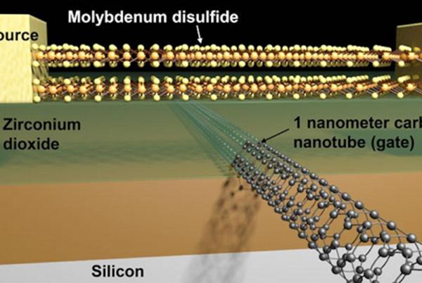
Silicon transistors keep shrinking (current state of the art is about 20 nanometers). However–in theory–once the gate goes to 5 nanometers, the electrons tunnel through the channel making it impossible to turn the transistor off. Berkeley researchers have used a different material to produce a transistor with a 1-nanometer gate. For point of reference, a human hair is about 50,000 nanometers thick.
The secret is to switch away from silicon in favor of another semiconductor. The team’s choice? Molybdenum disulfide. Never heard of it? You can buy it at any auto parts store since it is a common lubricant. Electrons have more effective mass as they travel through molybdenum disulfide than silicon. For a larger transistor, that’s not a good thing, but for a small transistor, it prevents the electron tunneling problem.
The history of the diode is a fun one as it’s rife with accidental discoveries, sometimes having to wait decades for a use for what was found. Two examples of that are our first two topics: thermionic emission and semiconductor diodes. So let’s dive in.
Vacuum Tubes/Thermionic Diodes
Our first accidental discovery was of thermionic emission, which many years later lead to the vacuum tube. Thermionic emission is basically heating a metal, or a coated metal, causing the emission of electrons from its surface.
Electroscope
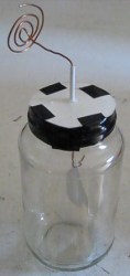
In 1873 Frederick Guthrie had charged his electroscope positively and then brought a piece of white-hot metal near the electroscope’s terminal. The white-hot metal emitted electrons to the terminal, which of course neutralized the electroscope’s positive charge, causing the leafs to come together. A negatively charged electroscope can’t be discharged this way though, since the hot metal emits electrons only, i.e. negative charge. Thus the direction of electron flow was one-way and the earliest diode was born.
Thomas Edison independently discovered this effect in 1880 when trying to work out why the carbon-filaments in his light bulbs were often burning out at their positive-connected ends. In exploring the problem, he created a special evacuated bulb wherein he had a piece of metal connected to the positive end of the circuit and held near the filament. He found that an invisible current flowed from the filament to the metal. For this reason, thermionic emission is sometimes referred to as the Edison effect.
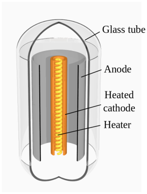
Thermionic diode. By Svjo [CC BY-SA 3.0], via Wikimedia CommonsBut it took until 1904 for the first practical use of the effect to appear. John Ambrose Fleming had actually consulted for the Edison Electric Light Company from 1881-1891 but was now working for the Marconi Wireless Telegraph Company. In 1901 the company demonstrated the first radio transmission across the Atlantic, the letter “S” in the form or three dots in Morse code. But there was so much difficulty in telling the received signal apart from the background noise, that the result was disputed (and still is). This made Fleming realize that a more sensitive detector than the coherer they’d been using was needed. And so in 1904 he tried an Edison effect bulb. It worked well, rectifying the high frequency oscillations and passing the signals on to a galvanometer. He filed for a patent and the Fleming valve, the two element vacuum tube or thermionic diode, came into being, heralding decades of technological developments in many subsequent types of vacuum tubes.
Vacuum tubes began to be replaced in power supplies in the 1940s by selenium diodes and in the 1960s by semiconductor diodes but are still used today in high power applications. There’s also been a resurgence in their use by audiophiles and recording studios. But that’s only the start of our history.
Psst… Wanna make a canning jar diode? A tennis ball triode? How about a semiconductor transistor? Or do you just enjoy sitting back and following along an interesting narrative of something being made, while picking up a wealth of background, tips and sparking all sorts of ideas? In my case I wanted to make a cuprous oxide semiconductor diode and that lead me to H.P. Friedrichs’ wonderful book Instruments of Amplification. It includes such a huge collection of amplifier knowledge and is a delight to read thanks to a narrative style and frequent hands-on experiments.
My well worn copy of Instruments of Amplifications
DIY point-contact semiconductor transistor
Friedrichs first authored another very popular book, The Voice of the Crystal, about making crystal radios, and wanted to write a second one. For those not familiar with crystal radios, they’re fun to make radios that are powered solely by the incoming radio waves; there are no batteries. But that also means the volume is low.
Readers of that book suggested a good follow-up would be one about amplifier circuits, to amplify the crystal radio’s volume. However, there were already an abundance of such books. Friedrichs realized the best follow-up would be one on how to make the amplifying components from scratch, the “instruments of amplification”. It would be unique and in the made-from-scratch spirit of crystal radios. The book, Instruments of Amplification was born.
The book includes just the right amount of a history, giving background on what an amplifier is and how they first came in the electrical world. Telegraph operators wanted to send signals over greater and greater distances and the solution was to use the mix of electronics and mechanics found in the telegraph relay. This is the springboard for his first project and narrative: the microphonic relay.
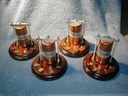
The microphonic relay example shown on the right places a speaker facing a microphone; the speaker is the input with the microphone amplifying the output. He uses a carbon microphone salvaged from an old telephone headset, housing everything in an enclosure of copper pipe caps, steel bar stock, nuts and bolts mounted on an elegant looking wood base. All the projects are made with simple parts, with care, and they end up looking great.
You can classify infrared light into three broad ranges: short wave, medium wave, and long wave. Traditionally, sensors concentrate on one or two bands, and each band has its own purpose. Short wave IR, for example, produces images similar to visible light images. Long wave is good for thermal imaging.
Researchers have announced a new detector that, by adjusting a bias, can detect all three bands using a simple approach that stacks different absorption layers over a semiconductor substrate. The device only requires two terminals and is very efficient, although the efficiency varies based on the band.
We’ve covered infrared sensing before. We’ve even seen DSLRs hacked into IR sensors. This new research might be a bit much to duplicate in your garage. After all, it requires tellurium doped gallium antimonide substrates and sophisticated processing equipment. However, this research will probably lead to practical devices that will find their way into projects before too long.
We’re all familiar with semiconductor devices, and we should remember the explanation from high-school physics classes that they contain junctions between two types of semiconductor material. “N” type which in the for-schoolchildren explanation has a surplus of electrons, and “P” type which has “Holes”, or a deficit of electrons.
Unless our careers have taken us deep into the science of the semiconductor industry though that’s probably as close as we’ve come to the semiconductors themselves. To us a diode or a transistor is a neatly packaged device with handy wires. We’ve never really seen what’s inside, let alone made any real semiconductor devices ourselves.
What makes his experiments particularly impressive though is not merely that he’s created a working diode, albeit one with a low reverse breakdown voltage. He’s done it not in a gleaming laboratory with a full stock of chemicals and equipment, but on his bench with a candle, and drops of water. He takes us through the whole process, with full details of his semiconductor manufacture as well as his diode test rig to trace the device’s I/V curve. Well worth a read, even if you never intend to make a diode yourself.
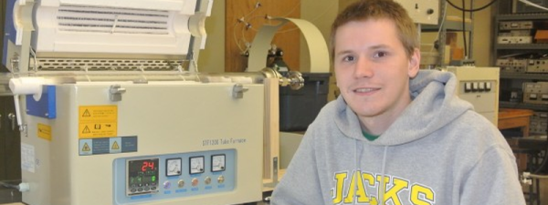
When you think of South Dakota you generally think of Mount Rushmore and, maybe, nuclear missiles. However, [Simeon Gilbert] will make you think of semiconductors. [Simeon], a student at South Dakota State University, won first place at the annual Sigma Xi national conference because of his work on a novel magnetic semiconductor.
The material, developed in collaboration with researchers from the nano-magnetic group at the University of Nebraska-Lincoln, is a mix of cobalt, iron, chromium, and aluminum. However, some of the aluminum is replaced with silicon. Before the replacement, the material maintained its magnetic properties at temperatures up to 450F. With the silicon standing in for some of the aluminum atoms, the working temperature is nearly 1,000F.
We find it interesting that the article mentions Maxim doesn’t need to scale — yet we often find Maxim parts in short supply. If TI were to acquire the company this could change for some Maxium parts. Still, this move looks a lot like TI trying to bolster its hold on the portions of the analog chip market which both companies currently occupy.
Already this year we’ve seen Dialog acquire Atmel, Avago acquire Broadcom, and the merger agreement between Freescale and NXP. We probably missed a few, and this has us wonder who is next. Let us know what you think in the comments below.