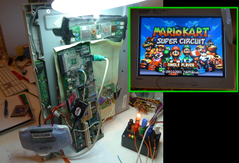
FPGAs, CPLDs, PALs, and GALs, Oh My! This week’s Hacklet focuses on some of the best Programmable Logic projects on Hackaday.io! Programmable logic devices tend to have a steep learning curve. Not only is a new hacker learning complex parts, but there are entire new languages to learn – like VHDL or Verilog. Taking the plunge and jumping in to programmable logic is well worth it though. High-speed projects which would be impossible with microcontrollers are suddenly within reach!
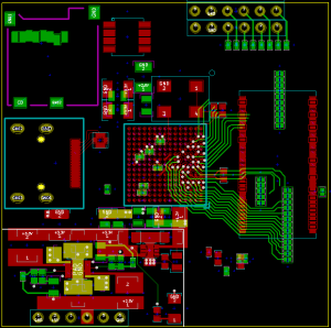 A great example of this is [Tom McLeod’s] Cheap FPGA-based HDMI Experimenting Board. [Tom’s] goal was to create a board which could output 720p video via HDMI at a reasonable frame rate. He’s using a Xilinx Spartan 6 chip to do it, along with a handful of support components. The images will be stored on an SD card. [Tom] is hoping to do some video with the setup as well, but he has yet to see if the chip will be fast enough to handle video decoding while generating the HDMI data stream. [Tom] has been quiet on this project for a few months – so we’re hoping that either he will see this post and send an update, or that someone will pick up his source files and continue the project!
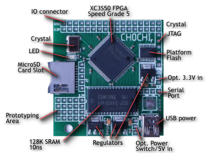
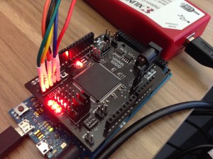 Next up is our own [technolomaniac] with his Arduino-Compatible FPGA Shield. Starting out with FPGAs can be difficult. [Technolomaniac] has made it a bit easier with this shield. Originally started as a project on .io and now available in The Hackaday Store, the shield features a Xilinx Spartan 6 FPGA. [Technolomaniac] made power and interfacing easy by including regulators and level shifters to keep the sensitive FPGA happy. Not sure where to start? Check out [Mike Szczys’] Spartan-6 FPGA Hello World! [Mike] takes us from installing Xilinx’s free tool chain to getting a “hello world” led blinker running!
 Still interested in learning about Programmable Logic, but not sure where to go? Check out [Bruce Land’s] Teaching FPGA parallel computing. Actually, check out everything [Bruce] has done on Hackaday.io – the man is a living legend, and a wealth of information on electronics and embedded systems. Being a professor of engineering at New York’s Cornell University doesn’t hurt either! In Teaching FPGA parallel computing, [Bruce] links to Cornell’s ECE 5760 class, which he instructs. The class uses an Altera/Terasic DE2 FPGA board to demonstrate parallel computing using programmable logic devices. Note that [Bruce] teaches this class using Verilog, so all you seasoned VHDL folks still can learn something new!
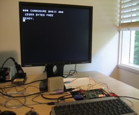
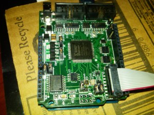 Finally, we have [Michael A. Morris] with Chameleon. Chameleon is an Arduino compatible FPGA board with a Xilinx Spartan 3A FPGA on-board. [Michael] designed Chameleon for two major purposes: soft-core processors, and intelligent serial communications interface. On the processor side Chameleon really shines. [Michael] has implemented a 6502 core in his design. This means that it would be right at home as the core of a retrocomputing project. [Michael] is still hard at work on Chameleon, he’s recently gotten fig-FORTH 1.0 running! Nice work [Michael]!
Want more programmable logic goodness? Check out our Programmable Logic List!
That about wraps things up for this episode of The Hacklet! As always, see you next week. Same hack time, same hack channel, bringing you the best of Hackaday.io!


