Exploring PC Floppy Protection: Formaster Copy-Lock

[GloriousCow] has started working on a series of investigations into the various historical floppy disk copy protection schemes used in the early days of the IBM PC and is here with the first of these results, specifically Formaster’s Copy-Lock.

This is the starting sector of track 6. It looks empty, but it’s not quite.

The game in question is King’s Quest by Sierra Entertainment, which used a ‘booter disk’ with the Copy-Lock protection scheme. Instead of having to boot DOS separately, you could just insert this disk and the game would launch automatically. Early copy protections often used simple methods, like adding sectors with non-standard sizes or tampering with sector CRC values to create disk errors. Copy-Lock employed several such tricks together, making it challenging for standard floppy disk hardware to replicate. In the case of Copy-Lock, Sector 1 on track 6 was intentionally written as only 256 bytes, with a 256-byte blank section to fill the gap. Additionally, the CRC was also altered to add another layer of protection.

When attempting to read the disk, the PC BIOS interrupt routine assumes it’s looking for a standard 512-byte sector, so when a “read sector” command is issued to locate the sector, it never finds it. To detect a dodgy copy, the game bypasses the BIOS and talks directly to the floppy disk controller using some custom code. The first part of the code uses the standard INT 13h routine to seek to track 6, sector 1, where it expects a fail since there is no valid sector there. Next, the floppy controller sends the “read track” command to perform a raw dump of all 512 bytes at this address and looks for a magic number, 0xF7, sitting in the final byte. That empty second half of the short sector is indeed not empty and is the check the game makes to determine if it was written with the Copy-Lock capable hardware. That last point is pertinent; you can’t create this disk structure with a standard IBM PC floppy disk controller; you need specialized hardware that can write different-sized sectors and incorrect CRCs, and that costs money to acquire.

We recently covered the copy protection scheme used for Dungeon Master on the Atari ST and the Amiga. If you’re thinking less about how a floppy got cracked and copied and more about how to preserve these digital relics, check this out!

Hardware Reuse: The PMG001 Integrated Power Management Module

Battery management is a tedious but necessary problem that becomes more of a hassle with lithium-ion technology. As we’re all very aware, such batteries need a bit of care to be utilized safely, and as such, a huge plethora of ICs are available to perform the relevant duties. Hackaday.IO user [Erik] clearly spent some time dropping down the same old set of ICs to manage a battery in their applications, so they created a drop-in castellated PCB to manage all this.

Continue reading “Hardware Reuse: The PMG001 Integrated Power Management Module”

Fast 3D Printing With A Polar, Four Quadrant Custom Machine

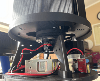
3D printing is all well and good for making low numbers of units, so long as they’re small enough to print in a reasonable time, but what if you want to go really big? Does a 35-hour print time sound like a fun time? Would it even make it that long? [Nathan] from Nathan Build Robots didn’t fancy the wait, so they embarked on a project to build a huge parallel 3D printer with four independent print heads. Well, kind of. Continue reading “Fast 3D Printing With A Polar, Four Quadrant Custom Machine”

A Simple 6DOF Hall Effect ‘Space’ Mouse

The 3DConnexion Space mouse is an interesting device but heavily patent-protected, of course. This seems to just egg people on to reproduce it using other technologies than the optical pickup system the original device uses. [John Crombie] had a crack at building one using linear Hall effect sensors and magnets as the detection mechanism to good — well — effect.

Using the SS49E linear Hall effect sensor in pairs on four sides of a square, the setup proves quite straightforward. Above the fixed sensor plate is a moveable magnet plate centred by a set of springs.  The magnets are aligned equidistant between each sensor pair such that each sensor will report an equal mid-range signal with zero mechanical displacement. With some simple maths, inputs due to displacements in-plane (i.e., left-right or up-down) can be resolved by looking at how pairs compare to each other. Rotations around the vertical axis are also determined in this manner.

Tilting inputs or vertical movements are resolved by looking at the absolute values of groups or all sensors. You can read more about this by looking at the project’s GitHub page, which also shows how the to assemble the device, with all the CAD sources for those who want to modify it. There’s also a detour to using 3D-printed flexures instead of springs, although that has yet to prove functional.

On the electronics and interfacing side of things, [John] utilises the Arduino pro micro for its copious analog inputs and USB functionality. A nice feature of this board is that it’s based on the ATMega32U4, which can quickly implement USB client devices, such as game controllers, keyboards, and mice. The USB controller has been tweaked by adjusting the USB PID and VID values to identify it as a SpaceMouse Pro Wireless operating in cabled mode. This tricks the 3DConnexion drivers, allowing all the integrations into CAD tools to work out of the box.

We do like Space Mouse projects. Here’s a fun one from last year, an interesting one using PCB coils and flexures, and a simple hack to interface an old serial-connected unit.


Using A 2D Scanner To Make 3D Things

[Chuck Hellebuyck] wanted to clone some model car raceway track and realised that by scanning the profile section of the track with a flatbed scanner and post-processing in Tinkercad, a useable cross-section model could be created. This was then extruded into 3D to make a pretty accurate-looking clone of the original part. Of course, using a flatbed paper scanner to create things other than images is nothing new, if you can remember to do it. A common example around here is scanning PCBs to capture mechanical details.

The goal was to construct a complex raceway for the grandkids, so he needed numerous pieces, some of which were curved and joined at different angles to allow the cars to race downhill. After printing a small test section using Ninjaflex, he found a way to join rigid track sections in curved areas. It was nice to see that modern 3D printers can handle printing tall, thin sections of this track vertically without making too much of a mess. This fun project demonstrates that you can easily combine 3D-printed custom parts with off-the-shelf items to achieve the desired result with minimal effort.

Flatbed scanner hacks are so plentiful it’s hard to choose a few! Here’s using a scanner to recreate a really sad-looking PCB, hacking a scanner to scan things way too big for it, and finally just using a scanner as a linear motion stage to create a UV exposure unit for DIY PCBs.

Continue reading “Using A 2D Scanner To Make 3D Things”

A Simple Guide To RF PCB Design

[Hans Rosenberg] knows a thing or two about RF PCB design and has provided a three-part four-part video demonstration of some solid rules of thumb. We will cover the first part here and leave the other two for the more interested readers!

The design process begins with a schematic diagram, assuming ideal conductors. Advanced software tools can extract the resistive, inductive, and capacitive elements of the physical wiring to create a parasitic model that can be compared to the desired schematic. The RF designer’s task is to optimize the layout to minimize differences and achieve the best performance to meet the design goals. However, what do you do when you don’t have access to such software?

[Hans] explains that at low frequencies, return current flows through all paths, with the lowest resistance path taking most of the current. At higher frequencies, the lowest inductance path carries all the current. In real designs, a ground plane is used instead of an explicit return trace for the lowest possible impedance.

You really wouldn’t design an RF circuit like this.

[Hans] shows the effect of interrupting the signal return path on a physical test PCB. The result is pretty bad, with the current forced to detour around the hole in the ground plane. A nanoVNA shows a -20 dB drop at 4 GHz, where the ground plane has effectively become an antenna. Energy will be radiated out, causing signal loss, but worse, it will create an EMC hazard with an unintended transmission.

Additionally, this creates an EMC susceptibility, making the situation worse. Placing a solder blob to bridge the gap directly under the signal trace is all that’s required to make it a continuous straight path again, and the performance is restored.

Floating planes are also an issue in RF designs, causing signal resonance and losses. One solution is to pull back the planes near the signal or stitch them to the ground plane with vias placed closely on either side of the signal trace. However, such stitching may slightly affect transmission line impedance and require tweaking the design a little. The next two parts of the series expand on this, hammering home the importance of good ground plane design. These are definitely worth a watch!

PCB design is as much art as science, and we’ve discussed this subject a lot. Here’s our simple guide to rocking RF PCB designs. There’s also a lot of devil in that detail, for example when understanding edge-launch SMA connectors.

Continue reading “A Simple Guide To RF PCB Design”

An Open Source 6kW GaN Motor Controller

We don’t know how you feel when designing hardware, but we get uncomfortable at the extremes. High voltage or current, low noise figures, or extreme frequencies make us nervous.  [Orion Serup] from CrabLabs has been turning up a few of those variables and has created a fairly beefy 3-phase motor driver using GaN technology that can operate up to 80V at 70A. GaN semiconductors are a newer technology that enables greater power handling in smaller packages than seems possible, thanks to high electron mobility and thermal conductivity in the material compared to silicon.

The KiCAD schematic shows a typical high-power driver configuration, broken down into a gate pre-driver, the driver itself, and the following current and voltage sense sub-circuits. As is typical with high-power drivers, these operate in a half-bridge configuration with identical N-channel GaN transistors (specifically part EPC2361) driven by dedicated gate drivers (that’s the pre-driver bit) to feed enough current into the device to enable it to switch quickly and reliably.

The design uses the LM1025 low-side driver chip for this task, as you’d be hard-pushed to drive a GaN transistor with discrete components! You may be surprised that the half-bridge driver uses a pair of N-channel devices, not a symmetric P and N arrangement, as you might use to drive a low-power DC motor. This is simply because, at these power levels, P-channel devices are a rarity.

Why are P-channel devices rare? N-channel devices utilise electrons as the majority charge carrier, but P-channel devices utilise holes, and the mobility of holes in GaN is very low compared to that of electrons, resulting in much worse ON-resistance in a P-channel and, as a consequence, limited performance. That’s why you rarely see P-channel devices in a circuit like this.

Continue reading “An Open Source 6kW GaN Motor Controller”