With a proliferation of USB Flash disk drives has come a very straightforward attack vector for a miscreant intent on spreading malware onto an organisation’s computer network. Simply drop a few infected drives in the parking lot, and wait for an unsuspecting staff member to pick one up and plug it into their computer. The drives are so familiar that to a non-tech-savvy user they appear harmless, there is no conscious decision over whether to trust them or not.
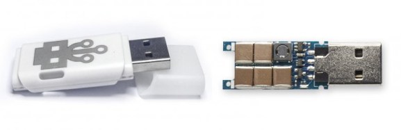
A diabolical variant on the exploit was [Dark Purple]’s USB Killer. Outwardly similar to a USB Flash drive, it contains an inverter that generates several hundred volts from the USB’s 5 volts, and repeatedly discharges it into the data lines of whatever it is plugged into. Computers whose designers have not incorporated some form of protection do not last long when subjected to its shocking ministrations.
Now the original has a commercial competitor, in the form of Hong Kong-based usbkill.com. It’s a bit cheaper than the original, but that it has appeared at all suggests that there is an expanding market for this type of device and that you may be more likely to encounter one in the future. They are also selling a test shield, an isolated USB port add-on that allows the device to be powered up without damaging its host.
From the hardware engineer’s point of view these devices present a special challenge. We are used to protecting USB ports from high voltage electrostatic discharges with TVS diode arrays, but those events have an extremely high impedance and the components are not designed to continuously handle low-impedance high voltages. It’s likely that these USB killers will result in greater sales of protection thermistors and more substantially specified Zener diodes in the world of USB interface designers.
We covered the original USB Killer prototype when it appeared, then its second version, and finally its crowdfunding campaign. This will probably not be the last we’ve heard of these devices and they will inevitably become cheaper, so take care what you pick up in that parking lot.
[via Extremetech]