Seeed Studio Shows Off Their Wares

Everyone’s favorite Open Hardware store – Seeed Studio – was at Maker Faire this last weekend. They showed off a bunch of cool toys, oscilloscopes, Arduino shields and other hardware goodness, but one of the more interesting products was from their B Squares line.

As [Colin] from Seeed showed us, each B Square is a small plastic enclosure about the size of a drink coaster. The corners of these squares are clad in metal, and each one has magnets inside. The idea behind the B Squares system is to provide power to other B Square boards via magnetic connections.

So far, Seeed has released an Arduino square, battery, solar, and LED squares, as well as iPod docks and prototyping boards. These boards can also be orthogonally, meaning it’s entirely possible to turn six B Squares into a B Cube.

These magnetic connections only provide power connections; there is currently no way to transfer data between different B Squares. We suspect, though, that anyone wanting to replicate the Apple MagSafe power adapter and invent a magnetic I2C bus would find these boards perfectly suited to the task.

Video after the break.

Continue reading “Seeed Studio Shows Off Their Wares”

Breadboarding With A 144-core Processor

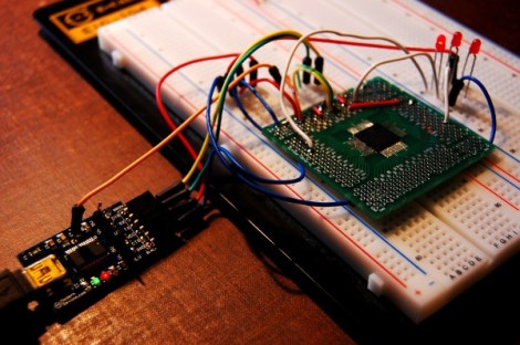
At the center of that green PCB is a tiny little processor with way too many cores. It’s the GA144 which was taken for a test-drive on a breadboard by [Andrew Back]. We saw a multi-core Kickstarter project last month. This will cost a lot less and get you more than twice the number of cores. But as was mentioned in the comments on that post, the drawback is the programming language. This chip’s IDE uses Forth.

There is a dev board available, but [Andrew] went instead with a QFN-to-Through-Hole adapter board which he hand soldered. Once he has access to the pins the chip can be programmed with an FTDI adapter which is compatible with the 1.8V logic levels. The provided Forth IDE (arrayForth) is a Windows only program but it does run under Wine. We followed the project through to see him twiddling I/O pins. But we still have trouble thinking of applications for it. In a world of complex and inexpensive FPGA chips, what would you use this type of processor for?

Checking In With [Ian] From Dangerous Prototypes

Former Hackaday writer and electronic wizard [Ian] from Dangerous Prototypes made his way to the Maker Faire last weekend. He had a ton of cool stuff to show off, and luckily we were able to grab a few videos.

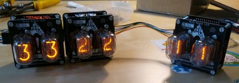
First up is a chainable Nixie module. [Ian], like all gurus of his caliber, had a box full of Nixie tubes waiting to be used in a project. These tubes never quite made it into their planned projects, mostly due to the difficulty of getting these old Nixies working. To remedy this problem, [Ian] created a chainable Nixie tube module – just hook up a high voltage supply to the board, connect it to the microcontroller of your choice, and you’ve got 2 Nixie tubes for your project.

[Ian] also showed off an ingenious solution to one of every maker’s problems. After designing a few cool boards like the Bus Pirate, Flash Destroyer, and Logic Sniffer, he realized he never made two boards that were the same size. This meant it was nigh impossible to have a standardized set of cases for his (and other maker’s) projects. The result is the Sick of Beige standard for electronics projects.

This standard provides PCB layouts in both square and golden rectangle formats complete with mounting holes, radiused corners, keepout areas, and suggested placement locations for USB ports and SD cards. The idea behind Sick of Beige is to get makers and fabbers using the same board dimensions so a set of standardized cases can be constructed. It’s an awesome idea and something we highly recommend for your next project.

Videos after the break.   Continue reading “Checking In With [Ian] From Dangerous Prototypes”

Massively Parallel Computer Costs $99

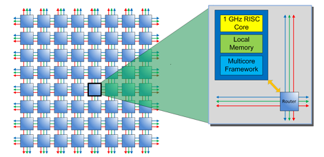
Even though dual, quad, and octo-core CPUs have been around for a while, it’s a far cry from truly massive parallel computing platforms. The chip manufacturer Adapteva is looking to put dozens of CPUs in a small package with their Parallella project. As a bonus, they’re looking for funding on Kickstarter, and plan to open source their 16 and 64-core CPUs after funding is complete.

The Parallella computer is based on the ARM architecture, and will be able to run Ubuntu with 1 Gig of RAM, a dual-core ARM A9 CPU, Ethernet, USB, and HDMI output. What makes the Parallella special is it’s Epiphany Multicore Accelerator – a coprocessor containing up to 64 parallel cores.

Adapteva is turning to Kickstarter for their Parallella computer to get the funding to take their Epiphany multicore daughterboard and shrink it down into a single chip. Once that’s complete, Adapteva will start shipping an ARM-powered Linux supercomputer that’s about the size of a credit card, or a Raspberry Pi under the new system of dev board measurements.

With any luck, the Parallella multicore computer will be available for $99, much less than a comparable x86 multicore computer. It’ll certainly be interesting to see what the Parallella can do in the future.

Volumetric Display Projects 200 Million Voxels Per Second

Over the last four years, [Will] and [Gav] have spent their time creating a huge, high-resolution 3D display. The’re just about done with their build, so they decided to offer it up to the Internet in the hopes of people creating new 3D content for their display. They call their project the HoloDome, and it’s the highest resolution volumetric display we’ve ever seen.

The HoloDome operates by spinning a translucent helix around its vertical axis at 20 rotations per second. A pico projector above the helix capable of projecting 1440 frames per second (an amazing device by itself) displays 72 ‘z-axis’ frames for each of the 60 ‘x and y frames’ per second. The result is a 3D display with a 480 * 320 * 72 voxel resolution capable of displaying 20 frames per second.

This isn’t the first time we’ve seen a swept helix used as a volumetric display, but it is by far the highest resolution display of its type in recent memory. [Gav] and [Will] have put their HoloDome up on the Australian crowd-funded site Pozible if you’d like to buy your own, but thankfully the guys have included enough detail on the main site to reconstruct this project.

Check out the video after the break to see the HoloDome in action.

Continue reading “Volumetric Display Projects 200 Million Voxels Per Second”

Homebrew FPGAs

Homebrew CPUs made out of logic chips are nothing new, but a homebrew FPGA is another matter entirely. [Joshua] sent in a project he whipped up where he made a single logic cell FPGA.

Despite how complicated and intimidating they are in practice, FPGAs are really very simple. They’re made of thousands of logic blocks capable of transmuting into AND, OR, NAND, and XOR logic gates. These logic blocks are all tied together, and with a somewhat complex hardware design language are capable of becoming a CPU, a micocontroller, or even a video card. Basically, programming a microcontroller tells a chip what to do, while programming an FPGA tells the chip what to be.

To build his single logic block FPGA, [Joshua] used a four-bit multiplexer to hard wire a truth table out of a 74HC174 D-type flip-flop. A bit of Arduino code changes the state of the pins connected to the multiplexer allows for any combination of TRUE and FALSE to be calculated for AND, NAND or XOR logic functions.

Yes, it’s only a single logic block for an FPGA, and if this build were expanded to even a few hundred cells it would be gargantuan. Still, there’s no better way to learn the ins and outs of abstract hardware, so we’ll gladly tip our hat to [Joshua] and his homebrew FPGA.

Reading Bare NAND Flash Chips With A Microcontroller

NAND flash, the same memory chips found in everything from USB thumb drives to very expensive solid state disk drives, are increasingly common. As they (partially) serve as the storage for cellphones, Wiis, routers and just about every piece of consumer electronic devices, you’re probably surrounded by dozens of NAND chips at any one time.

[Sprite_tm], hacker extraordinaire, put up a build a few years ago where he was able to read the contents of NAND Flash chips using a PC parallel port. It’s getting rather hard to find a parallel port on a PC anymore, so he updated his build to read Flash chips off of a USB port.

There are two main components of [Sprite_tm]’s build. First, to read the Flash chip, he needed a way to break out the pins on the very tiny TSOP48 package. [Sprite] found a neat little socket for these chips on eBay for about 10 Euros.

Communicating with the Flash chip via USB was a little harder. [Sprite] knew he needed USB 2.0, but not many microcontrollers have that implemented. Luckily, the FTDI FT2232H has USB 2.0, along with the very nice feature of being able to read data and address pins directly from the Flash chip. After a bit of soldering, [Sprite_tm] was left with the device seen above.

[Sprite_tm] found a nice library to bitbang the pins on the FTDI chip and request one page of memory from the Flash chip at a time. The device works as advertised, but it’s still a bit slow at 250 kBps. [Sprite] figures he can increase the speed of reading a Flash chip by requesting multiple pages at a time, but it’s still orders of magnitude faster than the old parallel port solution.

There’s a good bit of software [Sprite] posted to help him (and possibly others) read bare NAND flash chips via USB. This means if you have a broken USB Flash drive or SD card, it’s possible to desolder the chip and read it with your own controller. Interpreting the blocks of data recovered from a Flash drive as a file system is another story, but it’s still a fairly remarkable build.