Global Village Construction Set

The Global Village Construction Set is an open hardware initiative aimed at sharing tool-building knowledge. They believe that to build civilization you need forty basic tools, eight of which they’ve already prototyped and made available on their wiki. Included in these is a tractor which reminds us of a beefy bobcat. It has a soil pulverizing attachment which can be used to break down soil and feed it to their soil brick compressor. That machine spits out compressed dirt bricks which are used as building materials. They’re stacked on concrete footings and then limewashed to protect the un-baked bricks from water erosion. Does this remind anyone else of real-life Minecraft?

Above you can see a group of Open Source Ecology developers showing off bricks in front of the machine that made them, with the tractor/soil pulverizer to the right. Take a look at the videos about the construction set and brickmaking after the break. And learn more by perusing their weblog.

If you think an apocalypse is on the way you might want to buddy-up with these folks. They seem to know what they’re doing.

Continue reading “Global Village Construction Set”

Direct To PCB Inkjet Printing

[Rhys Goodwin] has been working on a system to print resist onto copper clad using an inkjet printer. This is a toner transfer alternative as it still uses toner, just not quite as you’d expect. The first step is to modify an inkjet printer, separating the carriage from the feed rollers in order to increase the clearance for the substrate. Instead of printing with etch resistant ink, as we’ve seen before, [Rhys] prints with black ink and then covers the board (ink still wet) in laser toner. Once there’s good adhesion he blows off the excess and bakes the board in a sandwich press, with spacers to keep the iron from touching the surface of the copper clad. This cooks the resist into a hard plastic layer and the board is ready for the acid. Watch him walk you through the process after the break.

[Rhys] uses the same method for silk screen, printing in red and baking the ink onto the substrate without added toner. This produces a nice looking board but it’s still quite a bit of work. It certainly sheds more light on the process than that laser-printer method from back in May. We hope you’ve been inspired by this and come up with the next innovation that makes this process easier.

Continue reading “Direct To PCB Inkjet Printing”

Test Beds And Jigs With Pogo Pins

Pogo pins – spring-loaded pin contacts are pretty fun to play with and even cooler when they get used in electronic devices like Adafruit and SparkFun’s test jigs. Check after the break for how these two companies have created their own production hacks. Continue reading “Test Beds And Jigs With Pogo Pins”

UV EPROM Eraser In A Toolbox

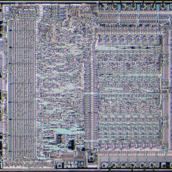
[Devon Croy] belongs to a hackerspace that works hard to keep hardware from going to the landfill. He found they were in possession of over a hundred Erasable Programmable Read Only Memory chips (EPROM). Not to be confused with EEPROM, which are electronically erasable, these EPROM chips require a strong source of UV light to blank the old data before they can be written again.

Instead of buying a tool to erase two or three chips at a time he built his own bulk EPROM eraser from an old metal toolbox. He used parts from a fluorescent black light and acquired a new bulb that generates light in the UVC spectrum, the band which works as an eraser for the chips. After bolting the parts into the case he added a spring-loaded timer knob and a safety switch that kills the power when the case is opened, similar to the UV exposure box we looked at yesterday.

Of course, if you don’t need a bulk eraser you could shop some garage sales for a UV pacifier cleaner which can also erase EPROM chips.

AVR DDS Signal Generator Improvements

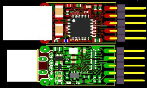
[Vassilis Papanikolaou] took a good thing and made it better with some design upgrades to this AVR based signal generator. We looked at version 1.0 of this tool back in 2006 and since then it saw an upgrade to 2.0. But [Vassilis] wanted to take things one step further, with a compact single-sided PCB. What you see above is the beautiful result of his work; a professionally made board that is compact, uses through-hole components, and has zero wire jumpers.

If you want to build one for yourself there’s a great parts list as well as board artwork and schematic. The system uses an ATmega16 so you’ll need a way to program one. There’s also just a bit of firmware tweaking to remap the control buttons to match the updated hardware layout.

Building A UV Exposure Box

There are two methods of using etchant resist when making circuit boards. We use the toner transfer method that requires ironing on laser toner to the copper, but you can also use chemical resist that reacts to ultraviolet light. [Bogdan] decided to start doing more of the latter so he built a UV exposure box to make the process easier.

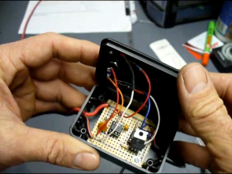
It is possible to use flourescent light bulbs for this, but he decided to use UV LEDs, a method we’ve also seen before. But there’s always room to innovate, and [Bogdan] built-in a couple of nice features that are new to us. Because the UV light can be bad for your eyes, he included a set of red visible-light LEDs on the bottom half of the box that are used to align two layers of exposure mask when making double-sided boards. There’s also a switch that automatically shuts off the UV light when the box is opened. And as the coup-de-grace, he added a programmable timer to regulate the exposure, using his newly created box when etching the PCB for it.

3D Printing With Visible Light

This 3D printer manages some pretty fantastic resolution, and these are just the early results of [Junior Veloso’s] build. He put together a machine that prints objects in resin that cures in visible light. To print, a thin layer of raw liquid resin self-levels across a printing surface and a DLP-based projector shines light from below, onto the portion to be hardened. The z-axis then pulls that layer up and the next to be printed will become the newest bottom layer. Horizontally the printer yields 1024×768 resolution with a layer thickness as small as 0.01 mm. No wonder he’s turning out this kind of quality.

The model above took 5 hours to print, with eight-second exposure for each layer, and 0.1mm layer thickness. There is lots of good information on his blog, from the early planning, to the finished hardware so take some time to learn about this fascinating project.

Update: Thanks to reader [Nave.notnilc] for pointing out that we’ve seen a chemical 3D printing technique before.