It’s common problem when you’re building anything with screws: this one is too long, this one is too short. While she can’t teach you how to fix the latter, [Quinn Dunki] has made herself an absolutely deluxe screw shortening jig. And while that’s cool and all, the real value here is the journey; watching over [Quinn]’s shoulders while she’s in the machine shop is always illuminating.
 First off, she starts with her old jig, which frankly makes us want one. It’s a short piece of aluminum angle stock with threaded holes in it. You thread the screw in as far as you want, and use the edge as a cutting guide. Very nice!
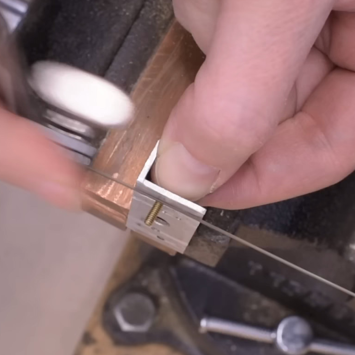
But aluminum threads wear out quickly so it works if you’re shortening dozens of screws, but gets wonky when you need to cut hundreds. The new jig is made out of steel, and has a slit that clamps the threads in place so she doesn’t have to hold the tiny screws with her other hand while sawing.
This video is, on the surface, about making an improved tool out of steel. But it’s the tips along the way that make it worth your watch. For instance “deburr early and often” is a recurring leitmotif here: it keeps the extra bits that form along any cut from messing up edge finding or vise registration. And yeah, she deburrs after every operation.
There are mistakes, and lessons learned along the way. We’re not going to spoil it all. But in the end, it’s a sweet tool that we’ve never seen before.
If you haven’t read [Quinn]’s series on machine tools that she wrote for us, it’s a treasure trove of machining wisdom.
Continue reading “[Quinn Dunki] Makes A Screw Shortener Fit For Kings”