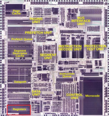
Intel’s 386 CPU is notable for being its first x86 CPU to use so-called standard cell logic, which swapped the taping out of individual transistors with wiring up standardized functional blocks. This way you only have to define specific gate types, latches and so on, after which a description of these blocks can be parsed and assembled by a computer into elements of a functioning application-specific integrated circuit (ASIC). This is standard procedure today with register-transfer level (RTL) descriptions being placed and routed for either an FPGA or ASIC target.
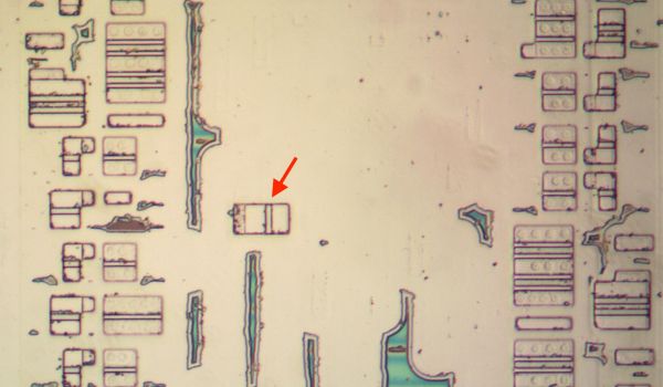
That said, [Ken Shirriff] found a few surprises in the 386’s die, some of which threw him for a loop. An intrinsic part of standard cells is that they’re arranged in rows and columns, with data channels between them where signal paths can be routed. The surprise here was finding a stray PMOS transistor right in the midst of one such data channel, which [Ken] speculates is a bug fix for one of the multiplexers. Back then regenerating the layout would have been rather expensive, so a manual fix like this would have made perfect sense. Consider it a bodge wire for ASICs.
Another oddity was an inverter that wasn’t an inverter, which turned out to be just two separate NMOS and PMOS transistors that looked to be wired up as an inverter, but seemed to actually there as part of a multiplexer. As it turns out, it’s hard to determine sometimes whether transistors are connected in these die teardowns, or whether there’s a gap between them, or just an artifact of the light or the etching process.


