An Unexpected Appearance Of An Iconic Motorola Chip

Big Clive's reverse-engineered schematic of the USB charger containing the MC34063 IC.
Big Clive’s reverse-engineered schematic of the USB charger containing the MC34063 IC.

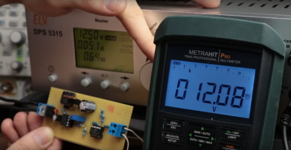
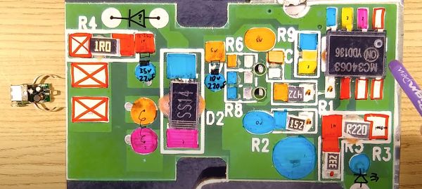
Generally when you crack open a cheap car-to-USB charger unit that came with some widget, you do not expect to find anything amazing inside. That’s why it was such a surprise to [Big Clive] when said car USB charger revealed a blast from the past in the form of an MC34063. This is a switching regulator that supports buck, boost and inverting topologies, but perhaps it most notable feature is that it was first produced by Motorola in the early 1980s.

This particular IC is marked as having been produced by ON Semiconductor which means that it’s technically still manufactured by Motorola – with ON Semiconductor being the Phoenix division that was spun off in 1999 – but it’s somewhat remarkable that this particular chip isn’t only produced by ON Semi today, but also by Texas Instruments. Much like the venerable NE555 timer IC and Intel’s 8051 MCU architecture, it would seem that certain chips and designs are simply made to become commodities in the future.

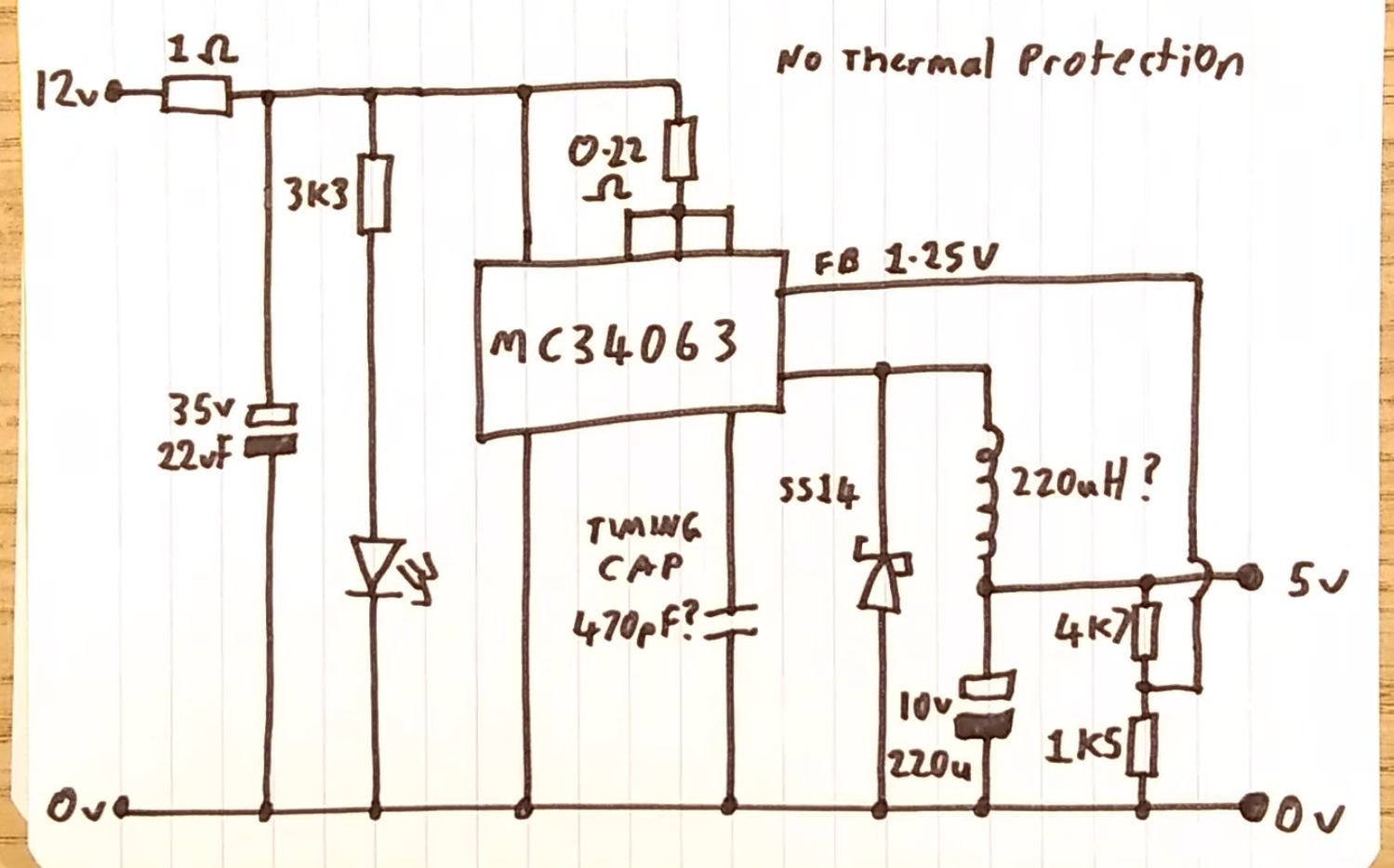
This appears to be the case for the MC34063 as well, which may lack some niceties of more modern ICs, such as built-in thermal protection, and it switches at only up to 100 kHz, but it can be bought for peanuts, has a wide input voltage range of 3 to 40 V, can switch up to 1.5 A and supports multiple common topologies. Often a 100 kHz switching regulator is all you need, in which case it’s handy to have a stack of such commodity chips lying around, plus the MC34063 comes in PDIP packaging as well, which is a boon for prototyping.

Continue reading “An Unexpected Appearance Of An Iconic Motorola Chip”

Bench Supplies Get Smaller Thanks To USB-C

Bench power supplies are an indispensable tool when prototyping electronics. Being able to set custom voltages and having some sort of current limiting feature are key to making sure that the smoke stays inside all of the parts. Buying a modern bench supply might be a little too expensive though, and converting an ATX power supply can be janky and unreliable. Thanks to the miracle of USB-C, though, you can build your own fully-featured benchtop power supply like [Brian] did without taking up hardly any space, and for only around $12.

USB-C can be used to deliver up to 100W but is limited to a few set voltage levels. For voltages that USB-C doesn’t support, [Brian] turns to an inexpensive ZK-4KX buck-boost DC-DC converter that allows for millivolt-level precision for his supply’s output. Another key aspect of using USB-C is making sure that your power supply can correctly negotiate for the amount of power that it needs. There’s an electronic handshake that goes on over the USB connection, and without it there’s not a useful amount of power that can be delivered. This build includes a small chip for performing this negotiation as well.

With all the electronics taken care of, [Brian] houses all of this in a 3D-printed enclosure complete with a set of banana plugs. While it may not be able to provide the wattage of a modern production unit, for most smaller use cases this would work perfectly. If you already have an ATX supply around, though, you can modify [Brian]’s build using that as the supply and case too.

Continue reading “Bench Supplies Get Smaller Thanks To USB-C”

The Negative Rail Explained

With the high availability of modular components and incredible wealth of information and tutorials online, it’s now easier than ever for hackers and makers to assemble complex electronic projects without getting bogged down with the theory behind it all. But the downside is that the modern electronic hobbyist often doesn’t have as deep an understanding of the low-level concepts that they would have if they had to build everything from scratch. This can be a problem when they try diagnosing and repairing faults, or when they start to branch out into reverse engineering.

Which makes “Building Blocks” by [David Christensen] a very compelling series. Every week he will be demonstrating a new circuit on his blog, complete with a plain English explanation of how and why it’s used. In this first installment of the series, he’s tackling a concept most of us have seen when poking around in more complex electronic devices, but maybe never really gave much thought to: the negative rail.

What exactly is the negative rail, anyway? It’s pretty easy to understand the positive rail in a circuit and its relation to ground; even multiple positive rails, such as in devices which use both 5 V and 3.3 V, are simple enough to wrap your head around. Unfortunately when something drops below that logical 0V reference, it isn’t quite as intuitive. But as [David] explains, the negative rail in a circuit is critical for dealing with bipolar signals, such as audio, which ride above and below the 0 V center point.

[David] goes over a few methods used to create the negative rail, from the classic center-tap transformer to using a buck-boost converter. But not content with just describing how these circuits work, he walks the reader through the creation of a charge pump circuit that you can drop into your next project if you find yourself in need of the elusive voltage. After explaining and diagramming it, he builds the circuit on a scrap piece of copper clad board and puts it through some benchmarks to prove it matches the theory he laid out.

If you’re in the mood for more negative talk, check out the battle our very own [Steven Dufresne] had with voltages of varying polarity when building his BB-8 robot.

Cleaning Up A Low-Cost Buck-Boost Supply

Cheap DC-DC converters have been a boon on the hobbyist bench for a while now, but they can wreak havoc with sensitive circuits if you’re not careful. The problem: noise generated by the switch-mode supply buried within them. Is there anything you can do about the noise?

As it turns out, yes there is, and [Shahriar] at The Signal Path walks us through a basic circuit to reduce noise from DC-DC converters. The module under the knife is a popular buck-boost converter with a wide input range, 0-32 VDC output at up to 5 amps, and a fancy controller with an LCD display. But putting the stock $32 supply on a scope reveals tons of harmonics across a 1 MHz band and overall ripple of about 66 mV. But a simple voltage follower built from a power op-amp and a Zener diode does a great job of reducing the spikes and halving the ripple. The circuit is just a prototype and is meant more as a proof of principle and launching point for further development, and as such it’s far from perfect. The main downside is the four-volt offset from the input voltage; there’s also a broad smear of noise at the high end of the spectrum that persists even with the circuit in place. Centered around 900 MHz as it is, we suspect a cell signal of some sort is getting in. 900 kHz.

If you haven’t checked out the videos at The Signal Path, you really should. [Shahriar] really has a knack for explaining advanced topics in RF engineering, and has a bench to die for. We’ve covered quite a few of his projects before, from salvaging a $2700 spectrum analyzer to multiplexing fiber optic transmissions.

Continue reading “Cleaning Up A Low-Cost Buck-Boost Supply”

A Buck-Boost Converter From The Ground Up

DC to DC conversion has come a long way. What was once took an electromechanical vibrator and transformer has been reduced to a PC board the size of a largish postage stamp that can be had for a couple of bucks on eBay. So why roll your own buck-boost converter for the ground up? Maybe because sometimes the best way to learn is by doing.

Continue reading “A Buck-Boost Converter From The Ground Up”