Chip Shortage Engineering: Misusing DIP Packages

After years of seeing people showing off and trading their badge Simple Add-Ons (SAOs) at Supercon, this year I finally decided to make one myself. Now for a first attempt, it would have been enough to come up with some cool PCB art and stick a few LEDs on it. But naturally I started with a concept that was far more ambitious than necessary, and before long, had convinced myself that the only way to do the thing justice was to have an onboard microcontroller.

My first thought was to go with the venerable ATtiny85, and since I already had a considerable stock of the classic eight-pin DIP MCUs on hand, that’s what I started prototyping with. After I had something working on the breadboard, the plan was to switch over to the SOIC-8 version of the chip which would be far more appropriate for something as small as an SAO.

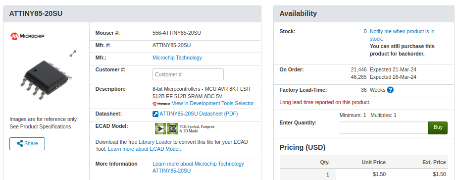
Unfortunately, that’s where things got tricky. I quickly found that none of the major players actually had the SMD version of the chip in stock. Both DigiKey and Mouser said they didn’t expect to get more in until early 2024, and while Arrow briefly showed around 3,000 on hand, they were all gone by the time I checked back. But that was only half the problem — even if they had them, $1.50 a piece seems a hell of a lot of money for an 8-bit MCU with 8K of flash in 2023.

The whole thing was made all the more frustrating by the pile of DIP8 ATtiny85s sitting on the bench, mocking me. Under normal circumstances, using them in an SAO wouldn’t really be a problem, but eight hand-soldered leads popping through the front artwork would screw up the look I had in mind.

While brooding over the situation my eyes happened to fall on one of the chips I had been fiddling with, it’s legs badly bent from repeated trips through the programmer. Suddenly it occurred to me that maybe there was a way to use the parts I already had…

Continue reading “Chip Shortage Engineering: Misusing DIP Packages”

Easyeda2KiCad: Never Draw A Footprint Again

What if I told you that you might never need to draw a new footprint again? Such is my friend’s impression of the tool that she’s shown me and I’m about to show you in turn, having used this tool for a few projects, I can’t really disagree!

We all know of the JLCPCB/LCSC/EasyEDA trio, and their integration makes a lot of sense. You’re expected to design your boards in EasyEDA, order the components on LCSC, and get the boards made by JLCPCB. It’s meant to be a one-stop shop, and as you might expect, there’s tight integration between all three. If there wasn’t, you’d be tempted to step outside of the ecosystem, after all.

But like many in this community, I use KiCad, and I don’t expect to move to a different PCB design suite — especially not a cloud one. Still, I enjoy using the JLCPCB and LCSC combination in the hobby PCB market as it stands now, and despite my KiCad affinity, it appears that EasyEDA can help me after all!

Continue reading “Easyeda2KiCad: Never Draw A Footprint Again”

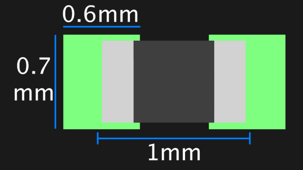
A graphic showing the suggested footprint dimensions for 0402 parts

Want Better 0402 Reflow? Consider These Footprints!

Assembling with a stencil is just that much more convenient – it’s a huge timesaver, and your components no longer need to be individually touched with a soldering iron for as many times as they have pads. Plus, it usually goes silky smooth, the process is a joy to witness, and the PCB looks fantastic afterwards! However, sometimes components won’t magically snap into place, and each mis-aligned resistor on a freshly assembled board means extra time spent reflowing the component manually, as well as potential for silent failures later on. In an effort to get the overall failure rate down, you will find yourself tweaking seemingly insignificant parameters, and [Worthington Assembly] proposes that you reconsider your 0402 and 0201 footprints.

Over the years, they noticed a difference in failure rates between resistor&capacitor footprints on various boards coming in for assembly – the size and positioning of the footprint pads turned out to be quite significant in reducing failure rate, even on a tenth of millimeter scale. Eagle CAD default footprints in particular were a problem, while a particular kind of footprint never gave them grief – and that’s the one they recommend we use. Seeing the blog post become popular, they decided to share their observations on 0201 as well, and a footprint recommendation too. Are your 0402 resistors giving you grief? Perhaps, checking the footprints you’re using is a good first step.

The 0402 and 0201 components are in a weird spot, where soldering iron assembly is no longer really viable, but the stencil+reflow approach might not be unilaterally successful when you start off – fortunately, that’s where writeups like these come in. Interested in learning stenciling? Get some solder paste, and read up on all the different ways you can put it onto your boards.

Autodesk Introduces Parametric Part Generation

The hardest part of any PCB design is adding parts and components. You shouldn’t use random part libraries, and creating your own part libraries is just a pain. Why have we endured this pain for so long, especially considering that most components follow a standard? Add in the fact that 3D modeling and rendering a board in a mechanical CAD tool is now a thing, making creating your own part libraries even more involved.

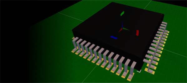
To solve this problem, Autodesk has introduced library.io, a tool to parametrically generate component footprints for Eagle and 3D models for Fusion360. Given that most parts follow a standard — QFP, TO-, DFN, or SOT23 — this is now the easiest way to create a new part in Eagle with its own 3D model that allows you to bring it into mechanical CAD tools.

An overview parametric parts generation is written up on the Autodesk forums, and covers what is possible with this new tool. There are actually two distinct versions, one is a web-based app that allows you to create packages and footprints parametrically in your browser and export them as a library. The other version of the tool is integrated with Eagle and allows you to create a new component parametrically from within Eagle.

This is a far cry from the standard method of creating new footprints. Instead of toiling over a datasheet and dropping correctly sized pads onto a grid, creating a new parametric footprint is as easy as copying a few numbers. In addition to the new parametric design feature, there’s a new tool in Eagle that does away with placing and naming pins for symbols. Now you can simply cut and paste a list of pins from the datasheet.

It should be noted that everything created with the library.io tool can be downloaded and used offline. Combine that with the recent news that KiCad can now ingest Eagle board and schematic files, and you have a way to create parametric footprints in everyone’s favorite Open Source PCB tool as well.