Today ahead of the Bay Area Maker Faire, Arduino has announced a bevy of new boards that bring modern features and modern chips to the Arduino ecosystem.
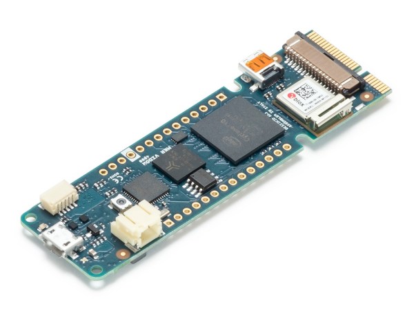
Most ambitious of these new offerings is a board that combines a fast ARM microcontroller, WiFi, Bluetooth, and an FPGA. All this is wrapped in a package that provides Mini HDMI out and pins for a PCIe-Express slot. They’re calling it the Arduino MKR Vidor 4000.
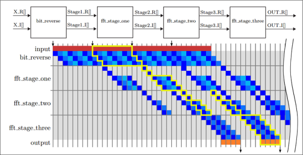
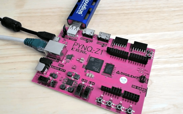
Bringing an FPGA to the Arduino ecosystem is on the list of the most interesting advances in DIY electronics in recent memory, and there’s a lot to unpack here. FPGA development boards aren’t new. You can find crates of them hidden in the storage closet of any University’s electronics lab. If you want to buy an FPGA dev board, the Terasic DE10 is a good starter bundle, the iCEstick has an Open Source toolchain, and this one has pink soldermask. With the release of the MKR Vidor, the goal for Arduino isn’t just to release a board with an FPGA; the goal is to release a tool that allows anyone to use an FPGA.
The key to democratizing FPGA development is Arduino’s work with the Arduino Create ecosystem. Arduino Create is the company’s online IDE that gives everyone the ability to share projects and upload code with Over-the-Air updates. The MKR Vidor will launch with integration to the Arduino Create ecosystem that includes a visual editor to work with the pre-compiled IP for the FPGA. That’s not to say you can’t just plug your own VHDL into this board and get it working; that’s still possible. But Arduino would like to create a system where anyone can move blocks of IP around with a tool that’s easy for beginners.
A Facelift for the Uno WiFi
First up is the brand new Arduino Uno WiFi. While there have been other boards bearing the name ‘Arduino Uno WiFi’ over the years, a lot has changed in the world of tiny radio modules and 8-bit microcontrollers over the past few years. The new Arduino Uno WiFi is powered by a new 8-bit AVR, the ATMega4809. The ATMega4809 is a new part announced just a few months ago, and is just about what you would expect from the next-generation 8-bit Arduino; it runs at 20MHz, has 48 kB of Flash, 6 kB of SRAM, and it comes in a 48-pin package. The ATMega4809 is taking a few lattices of silicon out of Microchip’s playbook and adds Custom Configurable Logic. The CCL in the new ATMega is a peripheral that is kinda, sorta like a CPLD on chip. If you’ve ever had something that could be more easily done with logic gates than software, the CCL is the tool for the job.
But a new 8-bit microcontroller doesn’t make a WiFi-enabled Arduino. The wireless power behind the new Arduino comes from a custom ESP-32 based module from u-blox. There’s also a tiny crypto chip (Microchip’s ATECC508A) so the Uno WiFi will work with AWS. The Arduino Uno WiFi will be available this June.
But this isn’t the only announcement from the Arduino org today. They’ve been hard at work on some killer features for a while now, and now they’re finally ready for release. What’s the big news? Debuggers. Real debuggers for the Arduino that are easy to use. There are also new boards aimed at Arduino’s IoT strategy.
Continue reading “Arduino Just Introduced An FPGA Board, Announces Debugging And Better Software” →

 So, how does it actually test? Synthesized inside the FPGA is everything the CPU needs from the motherboard to make it tick, including ROM, RAM, bus controllers, clock generation and interrupt handling. Many testing frequencies are supported (which is helpful for spotting fakes), and if connected to a computer via USB, the UCA can check power consumption, and even benchmark the chip. We can’t begin to detail the amount of thought that’s gone into the design here, from auto-detecting data bus width to the sheer amount of models supported, but you can read more technical details


