There is a chain of trust in every modern computing device that starts with the code you write yourself, and extends backwards through whatever frameworks you’re using, whatever OS you’re using, whatever drivers you’re using, and ultimately whatever BIOS, UEFI, Secure Boot, or firmware you’re running. With an Intel processor, this chain of trust extends to the Intel Management Engine, a system running independent of the CPU that has access to the network, USB ports, and everything else in the computer.
Needless to say, this chain of trust is untenable. Any attempt to audit every line of code running in a computer will only be met with frustration. There is no modern Intel-based computer that is completely open source, and no computer that can be verified as secure. AMD is just as bad, and recent attempts to create an open computing platform have met with frustration. [Bunnie]’s Novena laptop gets close, but like any engineering task, designing the Novena was an exercise in compromise. You can get around modern BIOSes, coreboot still uses binary blobs, and Libreboot will not be discussed on Hackaday for the time being. There is no modern, completely open, completely secure computing platform. They’re all untrustworthy.
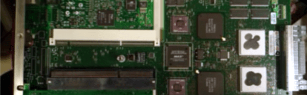
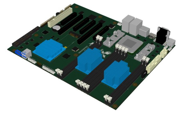
The Talos Secure Workstation, from Raptor Engineering, an an upcoming Crowd Supply campaign is the answer to the untrustworthiness of modern computing. The Talos is an effort to create the world’s first libre workstation. It’s an ATX-compatible motherboard that is fully auditable, from schematics to firmware, without any binary blobs.