The spectrum of laser technologies available to hackers has gradually widened from basic gas lasers through CO2 tubes, diode lasers, and now fiber lasers. One of the newer entries is the MOPA laser, which combines a laser diode with a fiber-based light amplifier. The diode’s pulse length and repetition rate are easy to control, while the fiber amplifier gives it enough power to do interesting things – including, as [Ben Krasnow] found, etch hologram-like diffraction gratings onto stainless steel.
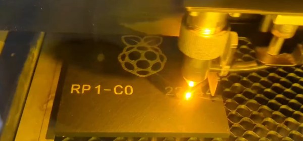
Stainless steel works because it forms a thin oxide layer when heated, with a thickness determined by the temperature it reaches. The oxide layer creates thin-film interference with incoming light, letting the laser mark parts of a steel sheet with different colors by varying the intensity of heating. [Ben] wrote a script to etch color images onto steel using this method, and noticed in one experiment that one area seemed to produce diffraction patterns. More experimentation revealed that the laser could consistently make diffraction gratings out of parallel patterns of oxide lines. Surprisingly, the oxide layer seemed to grow mostly down into the metal, instead of up from the surface.
The pitch of the grating is perpendicular to the direction of the etched lines, and varying the line spacing changes the angle of diffraction, which should in theory be enough control to print a hologram with the laser. [Ben]’s first experiment in this general direction was to create a script that turned black-and-white photographs into shimmering matrices of diffraction-grating pixels, in which each pixel’s grating orientation was determined by its brightness. To add a parallax depth effect, [Ben] spread out images into a gradient in a diffraction grating, so that it produced different images at different angles. The images were somewhat limited by the minimum size required for the grating pixels, but the effect was quite noticeable.
Unfortunately, since the oxide layers grow down into the metal, [Ben] doubts whether the laser can etch molds for diffraction-grating chocolate. If you’re interested in more diffraction optics, check out these custom diffraction lenses or the workings of normal holograms.