Woodcut Stamps And Conductive Ink

circuit

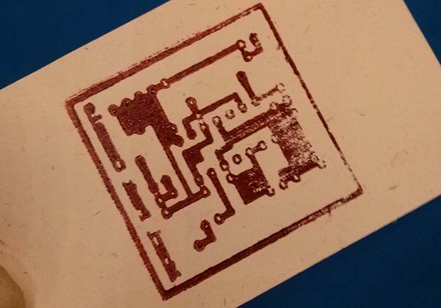
Even though it’s been a while since the Rome Maker Faire, we’re still getting some tips from the trenches of Europe’s largest gathering of makers. One of these is a 30-minute experiment from [Luong]. He wondered if it would be possible to create SMD circuit boards by using a 3D printer to fabricate a stamp for conductive ink.

[Luong] told this idea  to a few folks around the faire, and the idea eventually wound up in the laps of the guys from TechLab. the Chieri, Italy hackerspace. They suggested cutting a wooden stamp using a laser cutter and within 30 minutes of the idea’s inception a completed stamp for an Atari Punk Console PCB was in [Luong]’s hands.

As an experiment, the idea was a tremendous success. As a tool, the stamp didn’t perform as well as hoped; the traces didn’t transfer properly, and there’s no way this wooden laser cut stamp could ever create usable PCBs.

That being said, we’re thinking [Luong] is on the right track here with printed PCBs. One of the holy grails of home fabrication is the creation of printed circuit boards, and even a partial success is too big to ignore.

This idea for CNC-created PCB stamps might work with a different material – linoleum or other rubber stamp material, or even a CNC milled aluminum plate. If you have any ideas on how to use this technique for PCB creation, leave a note in the comments, or better yet, try it out for yourself.

Creating Irregular Board Outlines In KiCad

irregular-borders-in-kicad

One of the benefits of plain text file format is that you can go in and edit them by hand. This is part of the KiCad board outline hack which [Clint] wrote about in a recent post. He wanted a unique board outline, which is something that KiCad isn’t necessarily well suited for. His solution was to create the outline as an image, then import it. If you’re wondering what custom shape is called for this type of work we’d like to point you to the (kind of) bottle opening HaDuino. That PCB layout was done on Eagle, which has a bit more leeway with special shapes.

Before getting to the code editing step seen above [Clint] used the built-in feature for KiCad that will turn an image into a component. He exported that code and altered it using a text editor in order to change the layer setting for the shape to that of the board outline. This took him from a plain old image, to a module which can be selected and dropped into the board editing program. It’s a snap to do this sort of thing for the copper layers too if you’re interested in using your mad graphics editing skills to layout an art piece on copper clad.

Backlit PCB Panel As Wall Art

For his buddy’s wedding [Saar Drimer] wanted a one-of-a-kind gift, and what’s more unique than a piece of art? He set out to design something that would speak to his geeky game-loving friend. This full-panel PCB is what he came up with. It’s a wall hanging that uses addressable LEDs and a PCB for the enclosure and as a diffuser.

On the right you can see the panel as it was delivered to him. He used routed slots to separate the main body of the enclosure from the four side pieces and the mounting bracket. This design lets him snap off the parts and solder them in place. The only thing you need to add to it is a pair of screws (well, and the components that make it light up).

We’re shocked by how well the PCB works as a diffuser. The substrate is translucent when not covered with silk screen or the copper layers. The outline of the letters uses that, as well as circular areas along the side pieces. The letters themselves are copper fills that have artistic patterns removed from them. This really adds to the visual appeal when the piece is illuminated by 42 WS2812B LEDs. The video below shows the piece in action. It really takes PCB as art to the next level

Continue reading “Backlit PCB Panel As Wall Art”

Polyurethane Protecting PCBs

PCB

What you see above is a home-made PCB. No, this isn’t an example of a terrible toner transfer job, but rather evidence of the ravages of time. This board is seven years old, and the corrosion and broken traces show it. Luckily, [George] already has seven years of environmental data for a cheap DIY soldermask.

Seven years ago, [George] took a piece of copper clad board, masked half of it off, and sprayed it with fast drying polyurethane. After drying, he put it on a shelf in his garage. The results were fairly surprising – the uncovered portion is covered in verdigris, while the coated half is still shiny and new.

[George] took this a bit further and experimented with other spray can coverings. He found Testors spray enable worked just like the polyurethane, burning off when the heat of a soldering iron was applied, and also passed for a professional PCB.

PCB Agitator From A Broken CD-ROM Drive

pcb-agitator

Etching PCBs goes a lot better if you agitate the solution in order to carry away the dissolved copper and get fresh etchant to the area. With that in mind [Rohit Gupta] designed a mechanism in Sketch Up before realizing he was going about it the hard way. He ended up basing his agitator on a broken CD-ROM drive instead of starting from scratch.

He uses the CD sled from the drive, ditching the lens and its support structure. To get direct access to the motor that drives the tray he uses an L293D H-bridge chip. This is controlled by an MSP430G2231 microcontroller. The driver board seen in the upper right includes a voltage regulator, three status LEDs, and one user input switch. Once triggered, the sled will move back and forth, contacting an old mouse microswitch which acts as the limiting switch. We find it entertaining that [Rohit] prototyped the circuit on a breadboard, then used that success to etch the final circuit board (shown in the video below).

If you’ve been following the hacker creed and never getting rid of any junk you’ll have no problem finding a donor drive to make one of your own. But just in case you can’t get a hold of this hardware a similar agitator can be built using a hobby servo.

Continue reading “PCB Agitator From A Broken CD-ROM Drive”

Fail Of The Week: Motorizing A PCB Cutting Shear

This week’s fail is an attempt to retrofit a PCB cutting shear with a geared motor. The project was undertaken by [David Cook]. Incidentally he’s very near and dear to us as his book Robot Building for Beginners got us started with hacking in the first place.

This $200 shearing tool is hand-operated and can cut through boards up to 1/16″ thick. But [David] really had to crank on the thing to make a cut. This often resulted in crooked board edges. He decided to do the retrofit in order to achieve higher precision. He sourced a high-torque motor from eBay for around $50 delivered.

Continue reading “Fail Of The Week: Motorizing A PCB Cutting Shear”

Rock Solid PCB Mill Built At Home

Let’s all slow clap for [Daniel Taylor] who, after a long journey, got his home built PCB mill up and running with remarkable precision. That’s 10 mil traces with 0.5mm pitch pads. We’re impressed! The board will be used for breaking out the connections of an LCD screen he has on hand.

After seeing a CNC project as yesterday’s Fail of the Week it’s nice to look in on one like this that does some amazing stuff. In fact, [Daniel’s] creation has been working for months already. The link above is the project log he kept while hacking, tweaking, and retrofitting his rig to get the level of precision he was after.

Improvements include swapping out drawer slides for proper linear bearings and completely reworking the Z-axis along with a motor upgrade. For those that aren’t fans of the reading (how did you make it this far into this feature?) you can take a quick look at his image gallery which includes captions.