Reverse Engineering Salvaged Part Footprints

reverse-engineering-component-footprints

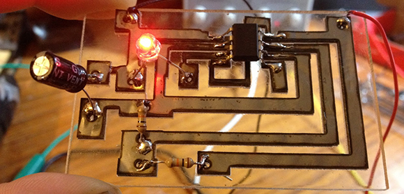
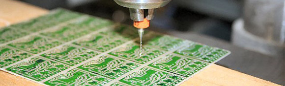
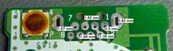
So you just pulled a fancy component off of a board from some broken electronics and you want to use it in your own project. What if the data sheet you found for it doesn’t include measurements for the footprint? Sure, you could pull out your digital calipers, but look at the measurements in the image above. How the heck are you supposed to accurately measure that? [Steve] found an easy answer for this problem. He uses microscope software to process an image of the board.

One common task when working with a microscope is measuring the items which are being viewed under magnification. [Steve] harnessed the power of a piece of free software called MiCam. One of its features is the ability to select an area of the photograph so serve as the measuring stick. To get the labels seen in the image above he selected the left and right edges of the board as the legend. He used his digital calipers to get a precise measurement of this area, then let the software automatically calculate the rest of the distances which he selected with his cursor.

MiCam is written for Windows machines. If you know of Linux or OSX alternatives please let us know in the comments.

Finding The Cheapest Board House

The prices for custom made circuit boards has never been cheaper, but surprisingly we’ve never seen a comparison of prices between the major board houses. [Brad] took the time to dig in to the price of 10 boards manufactured by Seeed Studios, OHS Park, and BatchPCB. He made some pretty graphs and also answered the question of where you can get your circuits made cheaply.

[Brad] got the prices for boards up to 20 cm x 20 cm from Seeed Studio’s Fusion PCB service, OSH Park, and BatchPCB. These results were graphed with Octave and showed some rather surprising results.

For boards over 20 cm2, the cheapest option is Seeed Studios. In fact, the price difference between Seeed and the other board houses for the maximum sized board is impressive; a 400 cm2 board from Seeed costs $150, while the same board from OSH Park is close to $1000.

Of course most boards are much smaller, so the bottom line is  for boards less than 20 cm2, your best bet is to go with OHS Park. If you don’t care when your boards arrive, or you need more than 10 or so, Seeed is the way to go. As far as the quality of the boards go, OSH Park is up there at the top as well.

Dead Motherboard Wall Hides An LED Marquee

dead-motherboard-led-marquee

[Jared] is a computer technician so he has no problem getting his hands on broken motherboards. It looks like he tends to save the more interesting colors and has finally found a use for the waste. He built this wall art which also acts as an LED marquee.

He came up with the size and shape — 18″ by 48″ — because it meshes well with a sheet of MDF. The outline allows for a grid made up of 2″ square pixels arranged seven high and twenty-one wide. The top and bottom rows will serve as a frame for the lights, which still leaves the five pixels necessary to display characters. From there he started wiring up the LED array, which is shown in the testing phase in the clip after the break. Each pixel is cordoned off by a frame of basswood which [Jared] fabricated on the table saw. The project is finished up by cutting the motherboards down to size and mounting them with threaded rod and nuts. The board chunks are not transparent but they’re smaller than the grid so the LEDs will make the edges glow.

This reminds us of the motherboards used to mimic stained glass from several years back.

Continue reading “Dead Motherboard Wall Hides An LED Marquee”

Laser Cut PCBs

19_done

Despite what you may have heard, those 40 Watt laser cutters actually can cut out traces on your next PCB.

Since he got his laser cutter a year and a half ago, [Rich] over at Nothing Labs has been trying to cut PCBs with it. Others have tried, usually by masking off a piece of copper followed by chemical etching. [Rich] wanted a one-step process, though, and his laser cutter really isn’t up to the task of cutting metal.

All that changed when he heard of another maker cutting  .001″ thick stainless steel on a similar laser cutter. Stainless steel isn’t solderable, but mild steel is. After finding a very thin piece of mild steel, [Rich] taped it down to a sheet of acrylic, designed a simple 555 blinky LED circuit, and tried out a new technique.

It turns out it is possible to cut very thin steel into circuit traces, and with enough flux to turn them into a functional circuit. As a bonus the resulting circuit looks really cool and a board can be made in mere minutes.

It’s not the thing for very fine work – the minimum trace width [Rich] can get is about 1/16″, but it is a very fast way to prototype a few circuits.

Continue reading “Laser Cut PCBs”

Humble Beginnings Of A Home Automation Project

humble-beginnings-to-a-home-automation-project

This board is the start of [Steven Pearson’s] quest to automate his home. The module will be used to prototype the rest of the project. Right now it uses an ATmega328 chip running the Arduino bootloader. This connects to one mechanical relay which we would wager is mains rated. The module will be controlled wirelessly via the wireless module seen in the foreground. That is a nRF24L01 board which he chose because of it’s bargain basement price tag of around $1.50.

There is much room for expansion in the system. You can see that a light-dependent resistor has been added to some of the microcontroller’s breakout pins. We would guess that [Steven] will use the hardware to develop for many different functions and will design more task-specific modules as the project progresses.

If you’re a fan of PCB milling and population you won’t want to miss the video after the break. [Steve] posted a fast-motion video of the entire process.

Continue reading “Humble Beginnings Of A Home Automation Project”

Letting [Euler] Help Out With PCB Fabrication

drillin

Since [Alessio] has been etching his own PCBs, he’s hit upon the most tedious part of the process, and the reason homebrew SMD boards are so awesome: drilling your own boards is a pain. While [Alessio]’s CNC mill takes care of most of the work, aligning the pre-drilled boards and correcting for any scaling issues from the mask is a bit difficult. With the help of a transform matrix, though, drilling PCBs has never been easier.

While the Gcode running the mill may be accurate, the actual manufactured PCBs might not be. If the extents on [Alessio]’s board aren’t exactly aligned with the axes of the CNC mill, the drill holes end up where they’re supposed to be. To solve this problem, [Alessio] wrote a PCB drilling transformational matrix calculator. The basic idea is by drilling just a few holes, [Alessio] is able to calculate any offset required in the Gcode with the help of a little bit of linear algebra.

Toner Transfer For Resist And Silk Screen Using Printable Vinyl

This toner transfer method uses a different material than we normally see. The red sheet being peeled back isn’t toner transfer paper. It’s printable vinyl used for both the resist and the silk screen.

The application process is almost the same as any other toner transfer PCB fabrication material. The printable vinyl stick is first adhered to a piece of paper before feeding it through a laser printer. It is acceptable to clean the vinyl with alcohol before printing if you think there may be a finger print or other oil on its surface. After printing it is carefully aligned with the board and ironed on.

[Mincior Vicentiu] thinks there are a few big benefits to this material. It seems that as you heat the toner it expands and hardens, but the vinyl actually softens to make room for this. We can imagine that this helps alleviate the smudging that sometimes occurs when ironing toner that is simply printed on paper. The other advantage is that the vinyl peels off quite easily after ironing, where as you need to soak paper in water and carefully massage it off of the toner.

[via Dangerous Prototypes]