With the successful arrival of China’s first Mars lander and rover this week, and the relatively recent addition of NASA’s Perseverance rover and its little helicopter sidekick Ingenuity, Mars has collected a lot of new hardware lately. But while the new kids on the block are getting all the attention, spare a thought for the reliable old warhorse which has been plying Gale Crater for the better part of a decade now — Curiosity. NASA has been driving the compact-car-sized rover around Mars for a long time now, long enough to rack up some pretty severe damage to its six highly engineered wheels, thanks to the brutal Martian rocks. But if you think Curiosity will get sidelined as its wheels degrade, think again — the rover’s operators have a plan to continue surface operations that includes ripping off its own wheels if necessary. It’s a complex operation that would require positioning the wheel over a suitable rock and twisting with the steering motor to peel off the outer section of the wheel, leaving a rim to drive around on. JPL has already practiced it, but they predict it won’t be necessary until 2034 or so. Now that’s thinking ahead.
With all the upheaval caused by the ongoing and worsening semiconductor shortage, it might seem natural to expect that manufacturers are responding to market forces by building new fabs to ramp up production. And while there seems to be at least some movement in that direction, we stumbled across an article that seems to give the lie to the thought that we can build our way out of the crisis. It’s a sobering assessment, to say the least; the essence of the argument is that 20 years ago or so, foundries thought that everyone would switch to the new 300-mm wafers, leaving manufacturing based on 200-mm silicon wafers behind. But the opposite happened, and demand for chips coming from the older 200-mm wafers, including a lot of the chips used in cars and trucks, skyrocketed. So more fabs were built for the 200-mm wafers, leaving relatively fewer fabs capable of building the chips that the current generation of phones, IoT appliances, and 5G gear demand. Add to all that the fact that it takes a long time and a lot of money to build new fabs, and you’ve got the makings of a crisis that won’t be solved anytime soon.
From not enough components to too many: the Adafruit blog has a short item about XScomponent, an online marketplace for listing your excess inventory of electronic components for sale. If you perhaps ordered a reel of caps when you only needed a dozen, or if the project you thought was a done deal got canceled after all the parts were ordered, this might be just the thing for you. Most items offered appear to have a large minimum quantity requirement, so it’s probably not going to be a place to pick up a few odd parts to finish a build, but it’s still an interesting look at where the market is heading.
Speaking of learning from the marketplace, if you’re curious about what brands and models of hard drives hold up best in the long run, you could do worse than to look over real-world results from a known torturer of hard drives. Cloud storage concern Backblaze has published their analysis of the reliability of the over 175,000 drives they have installed in their data centers, and there’s a ton of data to pick through. The overall reliability of these drives, which are thrashing about almost endlessly, is pretty impressive: the annualized failure rate of the whole fleet is only 0.85%. They’ve also got an interesting comparison of HDDs and SSDs; Backblaze only uses solid-state disks for boot drives and for logging and such, so they don’t get quite the same level of thrash as drives containing customer data. But the annualized failure rate of boot SDDs is much lower than that of HDDs used in the same role. They slice and dice their data in a lot of fun and revealing ways, including by specific brand and model of drive, so check it out if you’re looking to buy soon.
And finally, you know that throbbing feeling you get in your head when you’re having one of those days? Well, it turns out that whether you can feel it or not, you’re having one of those days every day. Using a new technique called “3D Amplified Magnetic Resonance Imaging”, or 3D aMRI, researchers have made cool new videos that show the brain pulsating in time to the blood flowing through it. The motion is exaggerated by the imaging process, which is good because it sure looks like the brain swells enough with each pulse to crack your skull open, a feeling which every migraine sufferer can relate to. This reminds us a bit of those techniques that use special algorithms to detects a person’s heartbeat from a video by looking for the slight but periodic skin changes that occurs as blood rushes into the capillaries. It’s also interesting that when we spied this item, we were sitting with crossed legs, watching our upper leg bounce slightly in time with our pulse.
Continue reading “Hackaday Links: May 16, 2021” →
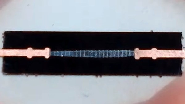
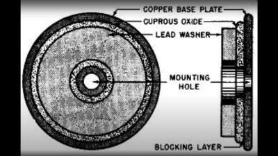 based not upon silicon or germanium, but copper. Copper (I) Oxide is a naturally occurring P-type semiconductor, which can be easily constructed by heating a copper sheet in a flame, and scraping off the outer layer of Copper (II) Oxide leaving the active layer below. Simply making contact to a piece of steel is sufficient to complete the device.
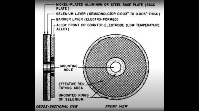 as the Selenium rectifier, based on the properties of a Cadmium Selenide – Selenium interface, which forms an NP junction, albeit one that can’t handle as much power as good old copper. One final device, which was a bit of an improvement upon the original CuO rectifiers, was based upon a stack of Copper Sulphide/Magnesium metal plates, but they came along too late. Once we discovered the wonders of germanium and silicon, it was consigned to the history books before it really saw wide adoption.