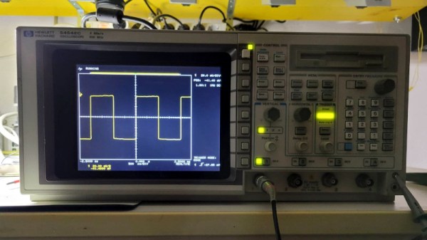
Although the HP 54542C oscilloscope and its siblings are getting on in years, they’re still very useful today. Unfortunately, as some of the first oscilloscopes to switch from a CRT display to an LCD they are starting to suffer from degradation. This has led to otherwise perfectly functional examples being discarded or sold for cheap, when all they need is just an LCD swap. This is what happened to [Alexander Huemer] with an eBay-bought 54542C.
Although this was supposed to be a fully working unit, upon receiving it, the display just showed a bright white instead of the more oscilloscope-like picture. A short while later [Alexander] was left with a refund, an apology from the seller and an HP 54542C scope with a very dead LCD. This was when he stumbled over a similar repair by [Adil Malik], right here on Hackaday. The fix? Replace the LCD with an FPGA and VGA-input capable LCD.
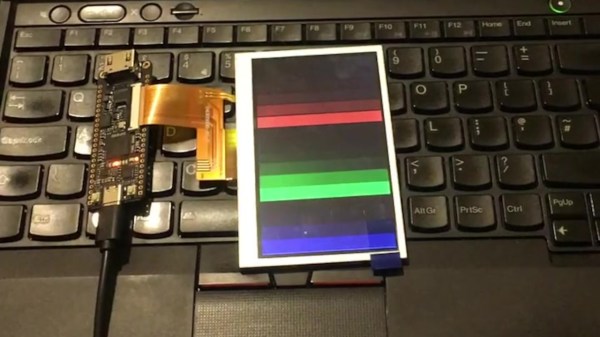
 While this may seem counter intuitive, the problem with LCD replacements is the lack of standardization. Finding an 8″, 640×480, 60 Hz color LCD with a compatible interface as the one found in this HP scope usually gets you salvaged LCDs from HP scopes, which as [Alexander] discovered can run up to $350 and beyond for second-hand ones. But it turns out that similar 8″ LCDs are found everywhere for use as portable displays, all they need is a VGA input.
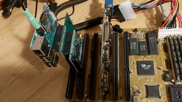
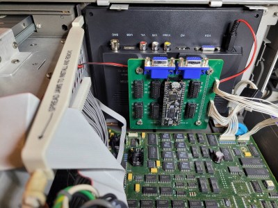
Taking [Adil]’s project as the inspiration, [Alexander] used an UPduino v3.1 with ICE40UP5K FPGA as the core LCD-to-VGA translation component, creating a custom PCB for the voltage level translations and connectors. One cool aspect of the whole system is that it is fully reversible, with all of the original wiring on the scope and new LCD side left intact. One niggle was that the scope’s image was upside-down, but this was fixed by putting the new LCD upside-down as well.
After swapping the original cooling fan with a better one, this old HP 545452C is now [Alexander]’s daily scope.