Aqueous Battery Solves Lithium’s Problems

The demand for grid storage ramps up as more renewable energy sources comes online, but existing technology might not be up to the challenge. Lithium is the most popular option for battery storage right now, not just due to the physical properties of the batteries, but also because we’re manufacturing them at a massive scale already. Unfortunately they do have downsides, especially with performance in cold temperatures and a risk of fires, which has researchers looking for alternatives like aqueous batteries which mitigate these issues.

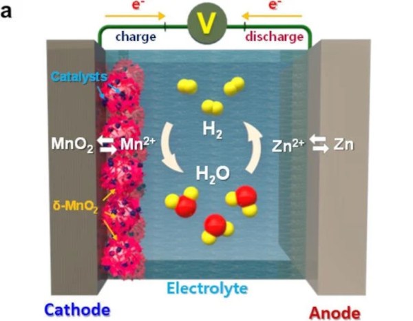
An aqueous battery uses a water-based electrolyte to move ions from one electrode to the other. Compared to lithium, which uses lithium salts for the electrolyte, this reduces energy density somewhat but improves safety since water is much less flammable. The one downside is that during overcharging or over-current situations, hydrogen gas can be produced by electrolysis of the water, which generally needs to be vented out of the battery. This doesn’t necessarily damage the battery but can cause other issues. To avoid this problem, researchers found that adding a manganese oxide to the battery and using palladium as a catalyst caused any hydrogen generated within the battery’s electrolyte to turn back into water and return to the electrolyte solution without issue.

Of course, these batteries likely won’t completely replace lithium ion batteries especially in things like EVs due to their lower energy density. It’s also not yet clear whether this technology, like others we’ve featured, will scale up enough to be used for large-scale applications either, but any solution that solves some of the problems of lithium, like the environmental cost or safety issues, while adding more storage to an increasingly renewable grid, is always welcome.

Open-Source Method Makes Possible Two-Layer PCBs With Through-Plating At Home

If the last year and its supply chain problems have taught us anything, it’s the value of having a Plan B, even for something as commoditized as PCB manufacturing has become. If you’re not able to get a PCB made commercially, you might have to make one yourself, and being able to DIY a dual-layer board with plated-through vias might just be a survival skill worth learning.

Granted, [Hydrogen Time]’s open-source method, which he calls “Process 01”, is something that he has been working on for years now. And it’s quite the feat of chemistry, which may require you to climb a steep learning curve, depending on how neglected the skills from high school or college chemistry are. But for as complex as Process 01 is, it’s actually pretty straightforward, and the first video below covers it in extreme detail. It starts with a drilled double-sided copper-clad board, which after cleaning is given a bath in palladium chloride. A follow-up dunk in stannous chloride leaves a thin film of palladium metal over all surfaces, even the via walls. This then acts as a catalyst for electroless copper plating in a solution of copper sulfate, followed by an actual electroplating step to thicken the copper plating.

After more washing, photoresist is applied to define the traces as well as to protect the now-plated vias, the board is etched, and a solder mask layer is applied. The boards might not be mistaken for commercial PCBs, but they’re pretty darn good, and as [Hydrogen Time] states, Process 01 is only a beginning. We expect this will be improved and streamlined as time goes by.

Fair warning, though — some steps require a fume hood to be performed safely. Luckily, we’ve got that covered. Sort of.

Continue reading “Open-Source Method Makes Possible Two-Layer PCBs With Through-Plating At Home”

Chemistry And Lasers Turn Any Plastic Surface Into A PCB

On the face of it, PCB production seems to pretty much have been reduced to practice. Hobbyists have been etching their own boards forever, and the custom PCB fabrication market is rich with vendors whose capabilities span the gamut from dead simple one-side through-hole boards to the finest pitch multilayer SMD boards imaginable.

So why on Earth would we need yet another way to make PCBs? Because as [Ben Krasnow] points out, the ability to turn almost any plastic surface into a PCB can be really handy, and is not necessarily something the fab houses handle right now. The video below shows how [Ben] came up with his method, which went down a non-obvious path that was part chemistry experiment, part materials science. The basic idea is to use electroless copper plating, a method of depositing copper onto a substrate without using electrolysis.

This allows non-conductive substrates — [Ben] used small parts printed with a Formlabs SLA printer — to be plated with enough copper to form solderable traces. The chemistry involved in this is not trivial; there are catalysts and surfactants and saturated solutions of copper sulfate to manage. And even once he dialed that in, he had to figure out how to make traces and vias with a laser cutter. It was eventually successful, but it took a lot of work. Check out the video below to see how he got there, and where he plans to go next.

You’ve got to hand it to [Ben]; when he decides to explore something, he goes all in. We appreciate his dedication, whether he’s using candles to explore magnetohydrodynamics or making plasma with a high-speed jet of water.

Continue reading “Chemistry And Lasers Turn Any Plastic Surface Into A PCB”

The Wedding Band: Milling Titanium And Wrapping It In Palladium

You’ve got to admit that custom milling your own wedding band is pretty hard-core. In this case [Jeremy Swerdlow] is making it for his friend, but that doesn’t diminish the fun of the project. After the break you can watch him mill a titanium ring and wrap it with a palladium inlay.

To solder palladium to titanium [Jeremy] would need special equipment, so he found another way to mate the dissimilar metals. He milled a dovetail groove in the center of the titanium band. To do that, he had to make a special cutting tool that was just the right size. Once had milled the ring’s rough dimensions, he had to fabricate a custom mandrel to hold the ring for the rest of the job. The dovetail was then filled with a palladium strip using a combination of heat and hammering. The two ends are soldered together using palladium solder. The ring in the middle shows this solder joint. To the right is a ring after the inlay is milled flush but before the final polishing which will bring out the best qualities of both metals.

If you don’t have the machine shop skills to pull this off you could always try your hand at 3d printed rings.

Continue reading “The Wedding Band: Milling Titanium And Wrapping It In Palladium”