Perovskites: Not Just For Solar Cells Anymore

If you’ve been around long enough, you’ll know there’s a long history of advances in materials science that get blown far out of proportion by both the technical and the popular media. Most of the recent ones seem to center on the chemistry of carbon, particularly graphene and nanotubes. Head back a little in time and superconductors were all the rage, and before that it was advanced ceramics, semiconductors, and synthetic diamonds. There’s always some new miracle material to be breathlessly and endlessly reported on by the media, with hopeful tales of how one or the other will be our salvation from <insert catastrophe du jour here>.

While there’s no denying that each of these materials has led to huge advancements in science, industry, and the quality of life for billions, the development cycle from lab to commercialization is generally a tad slower than the press would have one believe. And so when a new material starts to gain traction in the headlines, as perovskites have recently, we feel like it’s a good opportunity to take a close look, to try to smooth out the ups and downs of the hype curve and manage expectations.

Continue reading “Perovskites: Not Just For Solar Cells Anymore”

Self-Cleaning Camera Lens Makes For Speckle-Free Video

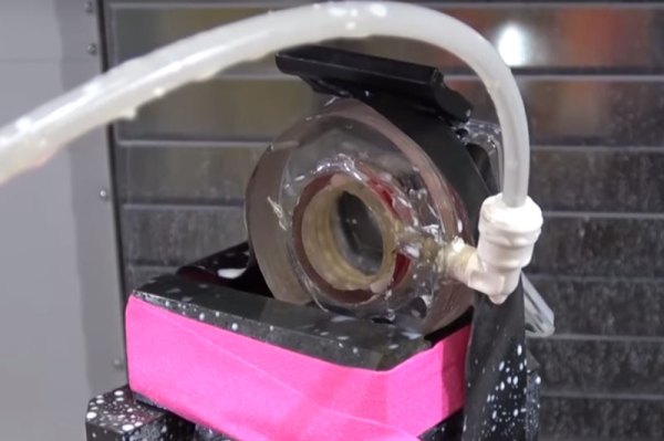
People making videos about machining have a problem: the coolant gets everywhere. When you take a video to show the process of creating a device, the milky gunk that keeps everything cool gets all over your camera lens. AvE is experimenting with an interesting fix for this problem, with a self-cleaning camera lens. (Video embedded below, some salty language.) His prototype uses a spinning piece of clear PVC mounted on BB gun pellets, driven by compressed air. The camera can see through this spinning piece, but when the coolant hits the spinning piece, it is thrown off.

Continue reading “Self-Cleaning Camera Lens Makes For Speckle-Free Video”

SOICbite: A Program/Debug Connector For An SOIC Test Clip

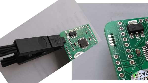
The problem is well-known: programming and debug headers consume valuable board space and the connectors cost money. Especially troublesome are the ubiquitous 100-mil pin headers, not because they’re expensive, but because they’re huge, especially along the z-axis. If you’re building miniature devices, these things can take up a ridiculous amount of space. With some clever thinking, [Simon Merrett] has found a way to re-use something many of us already have — an SOIC-8 test clip — to connect to a special footprint on the PCB without requiring another connector. He calls the system SOICbite.

The SOIC clip attaches to a footprint consisting of eight pads, four on each side of the PCB, plus five non-plated-through holes, which serve to anchor the clip in place. The idea of mating a PCB footprint directly with a removable connector isn’t entirely new — Tag Connect has been doing this for a while, but the connectors are expensive and single-sourced. On the other hand, SOIC test clips of varying quality are available from a number of vendors, including dirt-cheap deals on your favorite websites. The one disadvantage we can see is that the SOICbite footprint must be at the edge of the PCB to properly mate with the clip. The savings in space and cost may well make up for this, however.

[Simon] has made his KiCAD footprint available in a GitHub repo, and has offered to host footprints for any other CAD package there as well. So, fire up your preferred tool and draw one up for him to get these things widely adopted, because we think this is a great idea.

For the commercial alternative, check out our coverage of Tag Connect back in 2014.