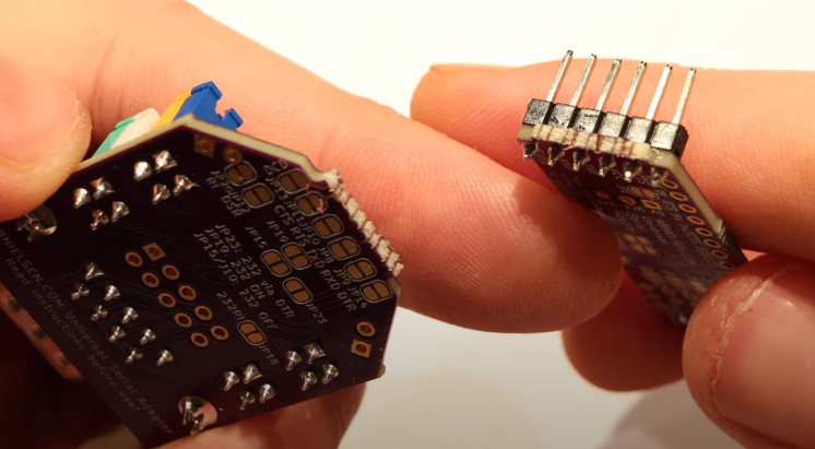
The Best DIY PCB Method?

Now before you start asking yourself “best for what purpose?”, just have a look at the quality of the DIY PCB in the image above. [ForOurGood] is getting higher resolution on the silkscreen than we’ve seen in production boards. Heck, he’s got silkscreen and soldermask at all on a DIY board, so it’s definitely better than what we’re producing at home.

The cost here is mostly time and complexity. This video demonstrating the method is almost three hours long, so you’re absolutely going to want to skip around, and we’ve got some relevant timestamps for you. The main tools required are a cheap 3018-style CNC mill with both a drill and a diode laser head, and a number of UV curing resins, a heat plate, and some etchant.

[ForOurGood] first cleans and covers the entire board with soldermask. A clever recurring theme here is the use of silkscreens and a squeegee to spread the layer uniformly. After that, a laser removes the mask and he etches the board. He then applies another layer of UV soldermask and a UV-curing silkscreen ink. This is baked, selectively exposed with the laser head again, and then he cleans the unexposed bits off.

In the last steps, the laser clears out the copper of the second soldermask layer, and the holes are drilled. An alignment jig makes sure that the drill holes go in exactly the right place when swapping between laser and drill toolheads – it’s been all laser up to now. He does a final swap back to the laser to etch additional informational layers on the back of the board, and creates a solder stencil to boot.

This is hands-down the most complete DIY PCB manufacturing process we’ve seen, and the results speak for themselves. We would cut about half of the corners here ourselves. Heck, if you do single-sided SMT boards, you could probably get away with just the first soldermask, laser clearing, and etching step, which would remove most of the heavy registration requirements and about 2/3 of the time. But if it really needs to look more professional than the professionals, this video demonstrates how you can get there in your own home, on a surprisingly reasonable budget.

This puts even our best toner transfer attempts to shame. We’re ordering UV cure soldermask right now.

Continue reading “The Best DIY PCB Method?”

2024 Business Card Challenge: Integrated Game Card

[Dan Schnur] has a simple strategy to ensure their business card stays on the client’s desk and doesn’t just get lobbed in a drawer: make it into a simple gaming platform. This entry into the 2024 Business Card Challenge is based around the tinyjoypad project, integrating an SSD1306 OLED display, joypad, and push button.

Powered by the superstar ATTiny85, the electronics are really not all that much, just a sprinkling of passives to support the display and the six switch inputs from the joystick and push button. Or at least, that’s how much we can glean from the PCB images, as the PCB design files are not provided in the project GitHub.

Leaving the heavy lifting of the software to the tinyjoypad project, the designer can concentrate on the actual job at hand and the reason the business card exists to stay at the forefront of the client’s mind. In the meantime, the card can be a useful distraction for those idle moments. A few such distractions include a tiny version of Missile Command (as shown above), tiny tris, and a very cut-down Q-bert.  Sadly, that last game isn’t quite the same without that distinctive sound.

Watch SLS 3D Printed Parts Become Printed Circuits

[Ben Krasnow] of the Applied Science channel recently released a video demonstrating his process for getting copper-plated traces reliably embedded into sintered nylon powder (SLS) 3D printed parts, and shows off a variety of small test boards with traces for functional circuits embedded directly into them.

Here’s how it works: The SLS 3D printer uses a laser to fuse powdered nylon together layer by layer to make a plastic part. But to the nylon powder, [Ben] has added a small amount of a specific catalyst (copper chromite), so that prints contains this catalyst. Copper chromite is pretty much inert until it gets hit by a laser, but not the same kind of laser that sinters the nylon powder. That means after the object is 3D printed, the object is mostly nylon with a small amount of (inert) copper chromite mixed in. That sets the stage for what comes next.

Continue reading “Watch SLS 3D Printed Parts Become Printed Circuits”

2024 Business Card Challenge: PCB Business Cards For Everybody

PCB business cards for electronics engineers might be very much old news in our circles, but they are still cool, not seen too much in the wild, and frankly inaccessible to those in other industries. For their entry into the 2024 Business Card Challenge, [Dima Shlenkevitch] is helping a little to alleviate this by providing a set of design examples and worked costs with suppliers.

Original green is still the cheapest option.

[Dima] lists key features every PCB business card should include, such as the expected thickness, restrictions for placing NFC components, and some aesthetics tips. Make sure to choose a supplier that allows you to remove their order number from the manufactured PCB, or it will look out of place.

Ordering PCBs with these specifications to keep costs reasonable requires effort, so [Dima] offers some example designs along with the results. If you want to have pretty gold lettering and graphics, you will need ENiG plating, increasing the price. Non-standard solder mask colors can also raise the price.

Will this help with the practical aspects of driving the PCB design software and actually placing the order? Obviously not, but the information provided gives you a leg up on some of the decisions so you don’t go down an expensive rabbit hole.

2024 Business Card Challenge: BAUDI/O For The Audio Hacker

[Simon B] enters our 2024 Business Card Challenge with BAUDI/O, a genuinely useful audio output device. The device is based around the PCM2706 DAC, which handles all the USB interfacing and audio stack for you, needing only a reference crystal and the usual sprinkling of passives. This isn’t just a DAC board, though; it’s more of an audio experimentation tool with two microcontrollers to play with.

The first ATTiny AT1614 is hooked up to a simple LED vu-meter, and the second is connected to the onboard AD5252 digipot, which together allows one to custom program the response to the digital inputs to suit the user. The power supply is taken from the USB connection. A pair of ganged LM2663 charge-pump inverters allow inversion of the 5V rail to provide the necessary -5 V for the output amplifiers.  This is then fed to the LM4562-based CMoy-type headphone amplifier.  This design has a few extra stages, so with a bit of soldering, you can adjust the output filtering to suit. An LM1117 derives 3.3 V from the USB input to provide another power rail,  mostly for the DAC.

There’s not much more to say other than this is a nice, clean audio design, with everything broken out so you can tinker with it and get exactly the audio experience you want.

2024 Business Card Challenge: T-800’s 555 Brain

In Terminator 2: Judgment Day it’s revealed that Skynet becomes self-aware in August of 1997, and promptly launches a nuclear attack against Russia to draw humanity into a war which ultimately leaves the door open for the robots to take over. But as you might have noticed, we’re not currently engaged in a rebellion against advanced combat robots.

The later movies had to do some fiddling with the timeline to explain this discrepancy, but looking at this 2024 Business Card Challenge entry from [M. Bindhammer] we think there’s another explanation for the Judgement Day holdup — so long as the terminators are rocking 555 timers in their chrome skulls, we should be safe.

While the classic timer chip might not be any good for plotting world domination, it sure does make for a great way to illuminate this slick piece of PCB art when it’s plugged into a USB port. Exposed copper and red paint are used to recreate the T-800’s “Brain Chip” as it appeared in Terminator 2, so even when the board isn’t powered up, it looks fantastic on display. The handful of components are around the back side, which is a natural place to put some info about the designer. Remember, this is technically supposed to be a business card, after all.

Continue reading “2024 Business Card Challenge: T-800’s 555 Brain”

An example of the case generated for a simple PCB, being shown in the OpenSCAD viewer

Turbocase Generates A PCB Shell For You

Our PCBs greatly benefit from cases – what’s with all the pins that can be accidentally shorted, connectors that stick out of the outline, and cables pulling the board into different directions. Designing a case for your PCB might feel like a fair bit of effort – but it likely isn’t, thanks to projects like turbocase from [Martijn Braam].

This script generates simple and elegant OpenSCAD cases for your KiCad PCBs – you only need to draw a few extra lines in the PCB Editor, that’s it. It makes connector openings, too – add a “Height” property to your connector footprints to have them be handled automatically. Oh, and there’s a few quality-of-life features – if your project has mounting holes, the script will add threaded-insert-friendly standoffs to the case; yet another argument for adding mounting holes to your boards, in case you needed more.

Installing the script is a single line, running it is merely another, and that will cover an overwhelming majority of boards out there; the code is all open too, of course. Want some more customization? Here’s some general project enclosure tutorials for OpenSCAD, and a KiCad-friendly StepUp tutorial. Oh, and of course, there’s many more ways to enclose PCBs – our own [Bob Baddeley] has written a guide to project enclosures that you are bound to learn new things from.

We thank [adistuder] for sharing this with us!