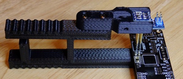
The new hotness for Internet of Things hardware is the ESP8266. Alone it can connect to a WiFi network, but it doesn’t really have a lot of output options. Paired with an ATMega, and you really have something. That’s the philosophy behind the WIOT board, and when [Chris] was assembling these boards, he needed a way to flash firmware. The board has an unpopulated ISP header from the assembler, so pogo pins are the answer. How do you make a pogo pin jig? With a 3D printer, of course.
The ISP header wasn’t populated to give the board a slim profile, but this means a jig of sorts would be needed to program the WIOT. The first attempt was buying a few pogo pin adapters from Tindie, but this was terribly uncomfortable to hold while the board was being programmed.
To fix this problem, a small clip device was rigged up, printed out, and used for programming. Interestingly, this clip has a very deep throat, and a few holes used for bolting on a separate programmer. This shows a lot of forward thinking: the programmer can be reused for different boards with completely different layouts and programmers. If the next revision of the WIOT needs a JTAG header to program the micro, the problem of programming it is already covered.

 While the most common use for a Raspberry Pi is probably a media center PC or retro game emulator, the Pi was designed as an educational computer meant to be an easy-to-use system in the hands of millions of students. Team 28 at Imperial College London certainly living up to the Raspberry Pi Foundation’s expectations