Last week on the Hacklet we covered optical microscopy projects. Those are the familiar scopes that many of us have at work or even at home on our benches. These are scopes that you typically can use with your eye, or an unmodified camera. This week we’re taking a look at more extreme ways of making small things look big. Electron streams and the forces of a single atom can be used to create incredibly magnified images. So let’s jump right in and check out the best advanced microscopy projects on Hackaday.io!
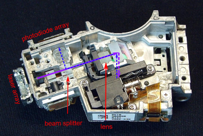 We start with [andreas.betz] and BluBEAM – a scanning laser microscope. [Andreas] aims to create a scanning confocal microscope. The diffraction limit is the law of the land for standard optical microscopes. While you can’t break the law, you can find ways around it. Confocal microscopy is one technique used quite a bit in medicine and industry. Confocal scopes are generally very expensive, well outside the budget of the average hacker. [Andreas] hopes to break that barrier by creating a scanning confocal microscope using parts from a PlayStation 3 Blu-Ray optical drive. Optical drives use voice coils to maintain focus. [Andreas] had to create a custom PCB with a voice coil driver to operate the PS3 optics assembly. He also needed to drive the laser. BluBeam is still very much a work in progress, so keep an eye on it!
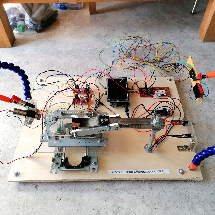
 Next up is [MatthiasR.] with DIY Scanning tunneling microscope. Open atmosphere scanning tunneling microscopes are popular on Hackaday.io. I covered [Dan Berard]’s creation in Hacklet 103. Inspired by Dan, [Matthias] is building his own STM.
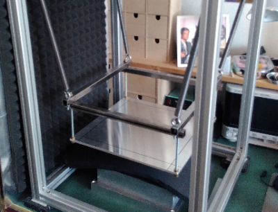
Environmental vibration is a huge problem with high magnification microscopes. [Matthias] is combating this by building a vibration isolation platform using extruded aluminum. He’s currently working on the STM preamplifier, which amplifies and converts the nano amp STM values to voltages which can be read by a digital to analog converter. [Matthias] is using the venerable Analog ADA4530 for this task. With an input bias of 20 femtoamps (!) it should be up to the task.
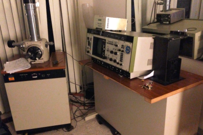 Next we have [Jerry Biehler] AKA [macona] with Hitachi S-450 Scanning Electron Microscope. Scanning electron microscopes have to be the top of the microscopy food chain. Jerry got his hands on a 1980’s vintage Hitachi SEM which was no longer working. The problem turned out to be a dodgy repair made years earlier with electrical tape. Fast forward a couple of years of use, and [Jerry] has done quite a lot to his old machine. He’s learned how to make his own filaments from tungsten wire. The slow oil diffusion vacuum pump has been replaced with a turbomolecular pump. The SEM now resides in [Jerry’s] living room, which keeps it at a relatively constant temperature.
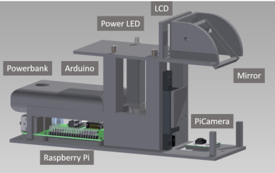 Finally, we have [beniroquai] with Holoscope – Superresolution Holographic Microscope. Holoscope is a device which increases the resolution of a standard camera by using the physical properties of light to its advantage. Precise tiny shifts of the object being magnified cause minute changes in a reflected image, which is captured by a Raspberry Pi camera. The Pi can then reconstruct a higher resolution image using the phase data. [beniroquai] has put a lot of time into this project, even sacrificing an expensive Sony connected camera to the ESD gods. I’m following along with this one. I can’t wait to see [beniroquai]’s first few images.
If you want to see more advanced microscopy projects, check out our new advanced microscope projects list! If I missed your project, don’t be shy, just drop me a message on Hackaday.io. That’s it for this week’s Hacklet. As always, see you next week. Same hack time, same hack channel, bringing you the best of Hackaday.io!