Of all the retro systems, the Commodore 64 had the best video system. The VIC-II chip in the C64 was the best example of why Commodore was the best, but in terms of video output, the C64 was still a consumer device: the only output was S-video, or composite video, or something like it. The professional stuff uses YPbPr, an RGB video signal that separates the red, green, and blue colors. On a modern LCD, the difference between composite and YPbPr is noticeable, and if you’re going to run your C64 on the big screen, it would be very helpful to use a professional video standard.
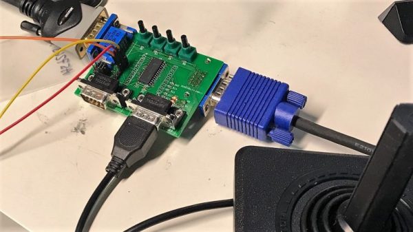
In an effort to bring the C64 into the future, [c0pperdragon] created an FPGA-based modification for the VIC-II chip. The end result is getting YPbPr signals directly from the computer, and outputting it to a TV in glorious 480p.
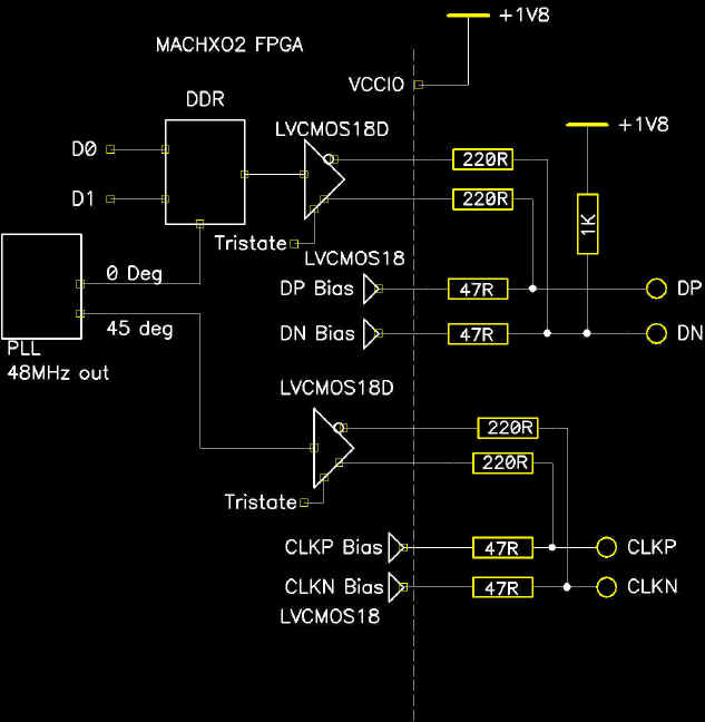
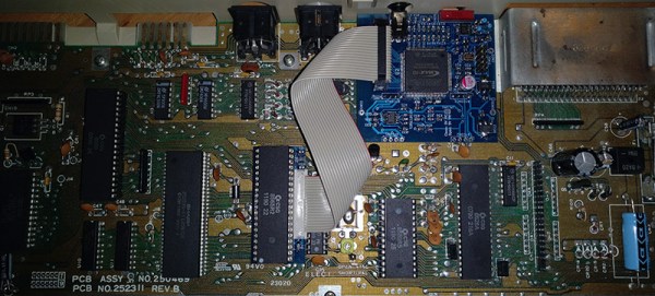
Inside the Commodore 64, the VIC-II creates the chrominance signal in a way that is impossible to convert it back to any form of RGB. The solution to get RGB out of this information is to listen in to 22 pins of the VIC-II to determine what signals it intends to generate. This is done with a smallish Altera FPGA connected to the VIC-II through a ribbon cable. On the FPGA, the luminescence and all the color information is generated, then converted into true YPbPr. For the complete mod, the RF modulator is removed, and the original A/V jack is still functional. This is effectively a very in-depth mod that rids the C64 of the TV connector and channel selector (that no one uses anymore) and replaces it with a professional-grade video output.
When it comes to C64 mods, we thought we’ve seen it all. We’ve seen C64s resurrected from the dead, and we’ve seen drop-in replacements for the SID that still don’t have working filters oh my god. This is on another level. This is using FPGAs to drag the C64 into the modern era, and if you don’t care about the rusting RF box, it’s a reversible mod.