It’s the 21st century, and according to a lot of sci-fi movies we should have perfected AI by now, right? Well we are getting there, and this project from a group of Cornell University students titled, “FPGA kNN Recognition” is a graceful attempt at facial recognition.
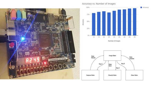
For the uninitiated, the K-nearest neighbors or kNN Algorithm is a very simple classification algorithm that uses similarities between given sets of data and a data point being examined to predict where the said data point belongs. In this project, the authors use a camera to take an image and then save its histogram instead of the entire image. To train the network, the camera is made to take mug-shots of sorts and create a database of histograms that are tagged to be for the same face. This process is repeated for a number of faces and this is shown as a relatively quick process in the accompanying video.
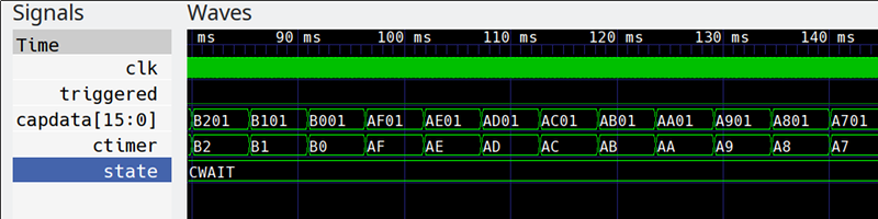
The process of classification or ‘guess who’, takes an image from the camera and compares it with all the faces already stored. The system selects the one with the highest similarity and the results claimed are pretty fantastic, though that is not the brilliant part. The implementation is done using an FPGA which means that the whole process has been pipe-lined to reduce computational time. This makes the project worth a look especially for people looking into FPGA based development. There is a hardware implementation of a k-distance calculator, sorting and selector. Be sure to read through the text for the sorting algorithm as we found it quite interesting.
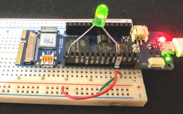
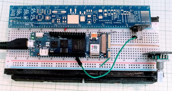
Arduino recently released the Arduino MKR4000 board which has an FPGA, and there are many opensource boards out there in the wild that you can easily get started with today. We hope to see some of these in conference badges in the upcoming years.