DIY USB Charging The Right Way

Since the widespread adoption of USB 1.1 in the 90s, USB has become the de facto standard for connecting most peripherals to our everyday computers. The latest revision of the technology has been USB 4, which pushes the data rate capabilities to 40 Gbit/s. This amount of throughput is mindblowing compared to the USB 1.x speeds which were three to four orders of magnitude slower in comparison. But data speeds haven’t been the only thing changing with the USB specifications. The amount of power handling they can do has increased by orders of magnitude as well, as this DIY USB charger demonstrates by delivering around 200 W to multiple devices at once.

The build comes to us from [tobychui] who not only needed USB rapid charging for his devices while on-the-go but also wanted to build the rapid charger himself and for the charger to come in a small form factor while still using silicon components instead of more modern gallium nitride solutions. The solution he came up with was to use a 24 V DC power supply coupled with two regulator modules meant for solar panel installations to deliver a staggering amount of power to several devices at once. The charger is still relatively small, and cost around $30 US dollars to make.

Part of what makes builds like this possible is the USB Power Delivery (PD) standard, which has enabled all kinds of electronics to switch to USB for their power needs rather than getting their power from dedicated, proprietary, and/or low-quality power bricks or wall warts. In fact, you can even use this technology to do things like charge lithium batteries.

Continue reading “DIY USB Charging The Right Way”

Can You Remembrandt Where This Is From?

A group of researchers have built an algorithm for finding hidden connections in artwork.

The team, comprised of computer scientists from MIT’s Computer Science and Artificial Intelligence Laboratory (CSAIL) and Microsoft, used paintings from the Metropolitan Museum of Art and Amsterdam’s Rijksmuseum to demonstrate these hidden connections, which link artwork that shares similar styles, such as Francisco de Zurbarán’s The Martyrdom of Saint Serapion (above left) and Jan Asselijn’s The Threatened Swan (above right). They were initially inspired by the “Rembrandt and Velazquez” exhibition in the Rijksmuseum, which demonstrated similarities between the artists’ work despite the former hailing from the Protestant Netherlands and the latter from Catholic Spain.

The algorithm, dubbed “MosAIc”, differs from probabilistic generative adversarial network (GAN)-based projects that generate artwork since it focuses on image retrieval instead. Rather than focusing solely on obvious factors such as color and style, the algorithm also tries to uncover meaning and theme. It does this by constructing a data structure called a conditional k-nearest neighbor (KNN) tree, which provides a tree-like structure where branches off a central image indicate similarity to the image. In order to query the data structure, these branches are followed until the closest match to an image in a dataset is found. In further iterations, it prunes unpromising branches in order to improve its time for new queries.

Some results from running the algorithm against museum collections were finding similarities between the Dutch Double Face Banyan and a Chinese ceramic figurine, traced to the flow of porcelain and iconography from the Chinese to the Dutch in the 16th to 20th centuries.

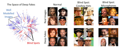
A surprising result of this study was discovering that the approach could also be applied to find problems with deep nerual networks, which are used for creating deepfakes. While GANs can often have blind spots in their models, struggling to recreate certain classes of photos, MosAIc was able to overcome these shortcomings and accurately reproduce realistic images.

While the team admits that their implementation isn’t the most optimized version of KNN, their main objective was to present a broad conditioning scheme that is simple but effective for applications. Their hope is to inspire related researchers to consider multi-disciplinary applications for algorithms.

Metasurface Design Methods Can Make LED Light Act More Like Lasers

Light-emitting diodes (LEDs) are not exactly new technology, but their use over time has evolved from rather dim replacements of incandescent signal lights in control panels to today’s home lighting. Although LEDs have the reputation of being power-efficient, there is still a lot of efficiency to be gained.

UC Santa Barbara researchers [Jonathan Schuller] and his team found that a large number of the photons that are generated never make it out of the LED. This means that the power that was used to generate these photons was essentially wasted. Ideally one would be able to have every single photon successfully make it out of the LED to contribute to the task of illuminating things.

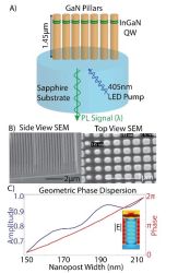
In their paper titled ‘Unidirectional luminescence from InGaN/GaN quantum-well metasurfaces‘  (pre-publication Arxiv version) they describe the problem of photon emission in LEDs. Photons are normally radiated in all directions, causing a ‘spray’ of photons that can be guided somewhat by the LED’s packaging and other parameters. The challenge was thus to start at the beginning, having the LED emit as many photons in one direction as possible.

Their solution was the use of a metasurface-based design, consisting out of gallium nitride (GaN) nanorods on a sapphire substrate. These were embedded with indium gallium nitride (InGaN) quantum wells which emit the actual photons. According to one of the researchers, the idea is based on subwavelength antenna arrays already used with coherent light sources like lasers.

With experiments showing the simulated improvements, it seems that this research may lead to even brighter, more efficient LEDs before long if these findings translate to mass production.

(Thanks, Qes)

The Amazing New World Of Gallium Nitride

From the heart of Silicon Valley comes a new buzzword. Gallium nitride is the future of power technology. Tech blogs are touting gallium nitride as the silicon of the future, and you are savvy enough to get in on the ground floor. Knowing how important gallium nitride is makes you a smarter, better consumer. You are at the forefront of your peer group because you know of an up and coming technology, and this one goes by the name of gallium nitride.

OK, gallium nitride is more than just a buzzword. It is, indeed, important materials science. Gallium nitride is a semiconductor that allows for smaller electronics, more powerful electric cars, better solar cells, and is the foundation of all LED lighting solutions today. Time will tell, but it may well mark a revolution in semiconductors. Here’s what you need to know about it now.

Continue reading “The Amazing New World Of Gallium Nitride”

Color-Tunable LEDs Open Up Possibilities Of Configurable Semiconductors

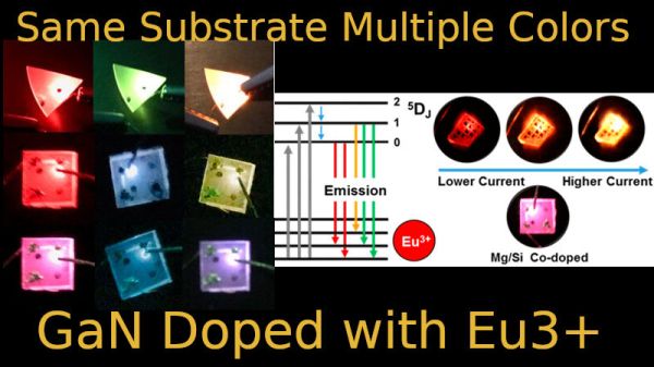
The invention of the blue LED was groundbreaking enough to warrant a Nobel prize. For the last decade, researchers have been trying to take the technology to the next level by controlling the color of emission while the device is in operation. In a new research paper, by the guys over Osaka University, Lehigh University, the University of Amsterdam and West Chester University have presented a GaN LEDs that can be tuned to emit different colors from the same substrate.

GaN or Gallium nitride is a wide band-gap semiconductor that has been employed in the manufacturing of FETs that are known to have higher power density due to its high thermal capacity while increasing efficiency. In the the case of the tunable LED, the key has been the doping with Europium for creating energy bands. When an electron jumps from a higher band to a lower band, it emits energy in the form of light and the wavelength or color depends on the gap of energy jumped as per Plank-Einstein equation.

By controlling the current density and duty cycle, the energy jumps can be controller thereby controlling the color being emitted. This is important since it opens up the possibility of control of LEDs post production. External controllers could be used with the same substrates i.e. same LEDs to make a lamp of different intensity as well as color without needing different doping for R,G and B emissions. The reduction in cost as well as size could be phenomenal and could pave the way for similar semiconductor research.

We have covered the details of the LED in the past along with some fundamentals on the control techniques. We are hoping for some high speed color accurate displays in the future that don’t break the bank on our next gaming build.

Thanks for the tip [Qes]

A Tesla Coil From PCBs

While at the Hacker Hotel camp in the Netherlands back in February, our attention was diverted to an unusual project. [Niklas Fauth] had bought along a Tesla coil, but it was no ordinary Tesla coil. Instead of the usual tall coil and doughnut-shaped capacity hat it took the form of a stack of PCBs with spacers between them, and because Tesla coils are simply cooler that way, he had it playing music as an impromptu MIDI-driven plasma-ball lousdpeaker. Now he’s been able to write up the project we can take a closer look, and it makes for a fascinating intro not only to double-resonant Tesla coils but also to Galium Nitride transistors.

The limiting factor on Tesla coils comes from the abilities of a transistor to efficiently switch at higher frequencies. Few designs make it above the tens of kHz switching frequencies, and thus they rely on the large coils we’re used to. A PCB coil can not practically have enough inductance for these lower frequencies, thus Niklas’ design employs a very high frequency indeed for a Tesla coil design, 2.6 MHz with both primary and secondary coils being resonant. His write-up sets out in detail the shortcomings of conventional MOSFETS and bipolar transistors in this application, and sets out his design choices in using the GaN FETs. The device he’s using is the TI LMG5200 GaN half-bridge driver, that includes all the necessary circuitry to produce the GaN FET’s demanding drive requirements.

The design files can be found in a GitHub repository, and you can see a chorus of three of them in action in the video below. Meanwhile [Niklas] is a prolific hardware hacker whose work has appeared on these pages in the past, so take a look at his ultrasonic phased array and his x-ray image sensor work.

Continue reading “A Tesla Coil From PCBs”

Open Source Power Converter For The Masses

GaN or Gallium Nitride Transistors have been in the news for their high-frequency and high-efficiency applications. Anyone interested in the Power Converter domain will love this open-source project by Siemens. The offering is called SDI TAPAS and it is a multipurpose GaN FET based board with a TMS320F28x controller onboard.

A quick look at the schematic reveals a lot of stuff going on like current and voltage sense chips along with a neatly designed GaN power stage with by-the-book drivers. There is a plethora of connectors on-board including one for the Raspberry Pi which is an added bonus. The git repository comes with sample code to get you off the ground, with examples running BLDC motors as well as connect it to Siemens MindSphere Cloud Platform.

This platform can be used in a number of functions in addition to motor control, such as battery charging, solar energy harvesting, and wireless charging. There is a presentation(PDF) that is available for download, and if you are looking for use cases there are a number of user build projects on their community site. The schematic and board designs can be used to make your own, or you could ask them for a sample board and they might give away more on their community site.

For those starting out, you might appreciate this tutorial on Buck Converter Efficiency to get a feel for the hardware that goes into such experiments.