Nanostructured metamaterials have shown a lot of promise in what they can do in the lab, but often have fatal stress concentration factors that limit their applications. Researchers have now found a strong, lightweight nanostructured carbon. [via BGR]
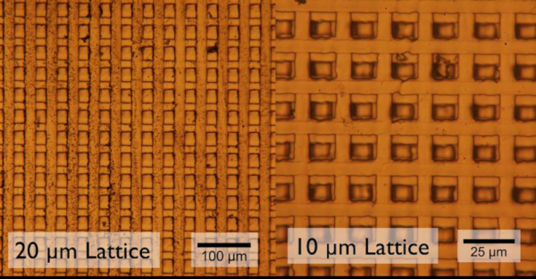
Using a multi-objective Bayesian optimization (MBO) algorithm trained on finite element analysis (FEA) datasets to identify the best candidate nanostructures, the researchers then brought the theoretical material to life with 2 photon polymerization (2PP) photolithography. The resulting “carbon nanolattices achieve the compressive strength of carbon steels (180–360 MPa) with the density of Styrofoam (125–215 kg m−3) which exceeds the specific strengths of equivalent low-density materials by over an order of magnitude.”
While you probably shouldn’t start getting investors for your space elevator startup just yet, lighter materials like this are promising for a lot of applications, most notably more conventional aviation where fuel (or energy) prices are a big constraint on operations. As with any lab results, more work is needed until we see this in the real world, but it is nice to know that superalloys and composites aren’t the end of the road for strong and lightweight materials.
We’ve seen AI help identify battery materials already and this seems to be one avenue where generative AI isn’t just about making embarrassing photos or making us less intelligent.


 In
In